Reply 200 of 753, by kool kitty89
feipoa wrote on 2019-12-26, 11:53:Was it the 32-bit external data bus which caused Intel such trouble in producing their socket 3 Pentium Overdrives?
I thought that was part of the matter, but more so that Intel tried to beef up performance to closer to Socket 5 levels (larger cache and other enhancements) and presumably didn't include variable bus sizing natively into the P5 or P54 architectures (I assume the 386 included native 16-bit bus support to allow the same dies for SX and DX production, and I know Motorola included viariable bus sizing support on the 68020, 030, 040, and 68EC000, with the latter including a 68008 style 8-bit bus configuration). Given the P54 made a number of other changes over the P5, it would've made more sense to think ahead and add that support natively too. (potentially simply by grounding one of the pins to enable 486 bus operation, though that would've allowed simple, cheap socket adapters too, which might not have been what Intel wanted, but they could always have left that pin disconnected in non-universal Overdrive type chips and/or could hardwire it internally, like with locked multipliers)
The Cyrix 5x86 was already a Socket 3/486 bus compatible part, so it should've been easier just to leave the existing I/O architecture in place and have the added 64-bit DRAM controller feed an internal latch tied to that 32-bit bus (and interface the external PCI I/O similar to Socket 3 boards through the media GX southbridge). Though honestly, I'd have thought it would've been simpler to not even bother with the integrated CPU and just refine the 5x86 core for IBM's 350 nm process and build an in-house embedded-system optimized Socket 3 chipset to go along with it. (potentially one that could go along with IBM's continued production of 5x86C surface-mounted chips)
An SiS style single-chip north+southbridge with integrated SVGA+sound support would've pretty well covered the Media GX feature set goals. They could've even cheaped out and omitted the board-level L2 cache controller and relied entirely on on-chip cache. (with the simpler chip, there'd be plenty of room for a 64kB L1 like the MX/M2 chips got, or Winchip) They wouldn't have to support other Socket 3 chips explicitly either, so potentially could do weird Cyrix-specific optimizations, too.
Sticking with the 486 bus interface would also mean a much smaller footprint for pins and traces for the CPU, including the 208 pin QFP used for 5x86 surface mounts. (though Socket 3 still offered the extended power and ground pins on the socket for an expanded PGA version, possibly better suited to higher CPU frequencies)
That's excluding a collaborate with VIA or SiS to develop such a chipset for a Socket 3 based interface. (SiS seems the obvious one given their existing integration efforts on top of the leading performance on late-gen Socket 3 chipsets and early Pentium chipsets)
For that matter, it might have even been cost-effective to bridge the 32-bit 6x86 bus onto a Socket 5/7 bus (I'm pretty sure that would just involve an intermediate 32 or 64-bit bus latch connected to the normal pentium bus interface) as a cheap, low power CPU for that platform, or as an inexpensive Socket 4 upgrade chip. (I suspect the original .65 micron 5x86 was reasonably tolerant of the native 5V Socket 4 interface unlike the AMD5x86's .35 micron process, while also being a fairly small chip compared to the P5 Pentium or .65 micron 6x86 in both die size and transistor count, so presumably wouldn't run all that hot at 5V and should also have had reasonable 133 MHz yields at the higher voltage, but would probably need the 5.25/5.27V boost disabled on boards that ran that at 66 MHz, also maybe 150 or 160 MHz support on boards with 50 or 40 MHz bus settings, like some of those nice SiS chipset boards)
I'd think the .65 micron 6x86 chips would have potential at 5V too, but they'd probably run a lot hotter than the P5 chips, might exceed the current supply limits of existing boards and need special heatsinks+fans, so probably not very attractive to socket 4 upgrades except maybe at 1x66 MHz. (where integer performance would still be a pretty nice step above the P5, but the really early 3-layer 650 nm chips might still pull too much current at 5V; I'm pretty sure the 5-layer interconnect versions allowed for a significantly smaller, denser die on the same 650 nm node size, so much less resistive losses across the die area)
I haven't seen delidded 3-layer and 5-layer 6x86s to compare, but the die lids themselves are noticeably different in size. (then again, the .35 and .65 5-layer parts seem to have pretty similar cover sizes, just with a less square cover and external resistors on the .35 chips: that goes for 2.8 and 3.5/3.3V rated parts, assuming CPUShack's ID guide is accurate, which also makes some sense given the 350 nm process should tolerate those voltages fine provided there's enough cooling, though it does make me wonder why AMD didn't service the 3.3/3.5V single-rail socket 5 market with the early model K6 unless they were just keeping the K5 in that role with existing stocks and production capacity investment and just leaving savvy, warranty-voiding users just overvolting Socket 7 chips on S5 boards, like with P55C)
Except I have seen the odd 3.3V core labeled K6/233 around on ebay listings, but maybe those were just oddball OEM parts specifically graded for such. (though I'm not sure running a 3.2V chip at 3.3V would even qualify a warranty violation as that seems within the typical margin)
Though I now wonder if the 3.5/3.3V .35 micron 6x86 chips are real single-rail chips or if they're identical to 6x86Ls other than the rating. (I don't have any of those myself, but it should be simple enough to test on a socket 7 board)
For that matter, I wonder if the 5x86 ever got a 5-layer revision or if the 3-layer process chip was small and efficient enough to stick with, or if that was one of the differences in IBM's 5x86C. (IBM also produced that for a long time, but I haven't seen any mention of a die-shrink, so presumably all of those still used the older 650 nm process)
Yeah, the MediaGX had 64-bit internal and external data buses, while the cx5x86 was 64-bit internal and 32-bit external. That 6 […]
wrote:Wait...MediaGX has a 64-bit datapath to memory? That really blows my mind.
Yeah, the MediaGX had 64-bit internal and external data buses, while the cx5x86 was 64-bit internal and 32-bit external. That 64-bit data bus to SDRAM didn't seem to help the MediaGX much in comparison to 32-bit FPM memory on a socket 3 though. The 33 MHz FSB must have been the crippling component.
On the cx5x86, that 64-bit data path is broken into two 32-bit paths to allow for some parallelism.
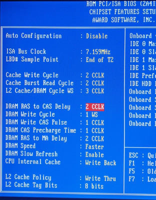
The cache data port is 64 bits wide and can be split into two 32-bit data paths. The ability to have two 32-bit data paths allows the 5x86 to simultaneously perform a 32-bit data transfer to or from main memory, and a 32-bit data transfer to or from the load/store unit.
I'd think the 64-bit cache data port would also accelerate cached FPU reads/writes as with the 64-bit external bus.
I also don't think the FSB on the Media GX actually refers to the DRAM interface at all, but the system I/O interface. The Ultimate 686 benchmark results showed consistent DRAM throughput gains as core multiplier settings and clock speeds ramped up and ended up exceeding the theoretical throughput of a 33 MHz FSB by a wide margin.
I didn't read the entire datasheet, but those results and the separate I/O (32-bit multiplexed, presumably locked at 33 MHz for PCI) and DRAM bus interfaces imply a separate clock rate is used for external DRAM. At a guess, maybe it's 1/3 the core clock speed, which would make the 180 MHz chips have a 60 MHz SDRAM clock and 200 MHz chips a 66 MHz one, and so on up to 100 MHz on 300 MHz chips. (that or the SDRAM clock divider varies with the multiplier setting automatically to avoid need for PC100 SDRAM, so 266 and 300 MHz core clocks would switch to x/4 for 66.6 and 75 MHz SDRAM clocks and 233 MHz core with 77.8 MHz SDRAM clock ... or maybe the SDRAM controller just runs at a fixed 2x the I/O bus speed, so always 60 or 66 MHz and not ties to the core clock at all other than both being multiplied from the same external source clock)
I'll have to check the spreadsheet again, but if the Media GX peaks below 533 MB/s throughput, that would be within the 66 MHz 64-bit memory clock spec.
I also assume they omitted FPM/EDO/BEDO DRAM support (in spite of the lower cost of that memory) due to SDRAM allowing a much simpler memory controller design while also offering high performance. (also probably banking on the cost of SDRAM coming down rapidly and making that investment pay off further)
Also, cache SRAM (especially simple asynchronous SRAM) should be pretty easily to interface externally through the DRAM port with a very simple external address latch to demultiplex the row/column lines to a linear 24-bit address (the Media GX has 12 physical DRAM address lines, though it has a 256Mbit or 32MB DRAM bank size limit) plus additional decoding of the DRAM bank select lines. However, since they omitted an on-chip cache controller, you'd need a full external L2 cache interface anyway, and including that latch would be relatively trivial (plus the multiplexed address lines would save on a few traces/pins, albeit not many compared to the 64 data lines), but that's still something Cyrix could've added as an optional external component for higher performing Media GX systems. (cache controller interface chip + asynch or pipeline burst SRAM onboard)
Given the small L1 cache size and bus contention when integrated video is used, an L2 cache should've made a big difference, especially as core clock speeds ramped up, even if that L2 cache was still accessed at the SDRAM clock frequency. (though bank-interleaving would at least reduce latency overhead for video accesses, so burst/page-mode cycles could be interrupted and re-started without the added overhead: this is one of the things that made shared system memory a headache on the N64 with the single 16-bit bank/channel of RDRAM and also a problem on some very early PC chipsets with integrated video memory, also the Atari Jaguar except sort of backwards there since the video/GPU ASIC is the only one capable of burst/page-mode bandwidth and the 68000 and DSP bus interfaces are both slower than even random memory cycle times; you also have some older home computers like the Amiga, Atari ST, some 8-bit computers, and I think the onboard video of the Tandy 1000 series that use interleaving within a single DRAM bank with the DRAM controller feeding bus latches and CPU+video DMA clocks synchronized to even/odd memory cycles; the Apple II used that approach without the use of latches I think, just with tight timing and the slowness of the 1 MHz 6502 and 500 ns DRAM cycles allowing a CPU access and video access within a single 1 MHz tick)
I think some fast, late model ISA VGA/SVGA cards might have used the old style of interleaved memory access too (allowing video memory access across the ISA bus during active display and/or simulating the EGA/VGA-native bank-interleaved bitplane addressing through a single, fast DRAM bank) while older cards were limited to bank-interleaving parallelism and slow cards might only allow access in vblank and a few cards using SRAM or PSRAM might allow easier parallelism, like ATi's Small Wonder. (and mode 13h displays block/saturate the 4 VGA banks, which I think restricts access to vblank on old/true VGA cards and MCGA with just the single 64kB bank)
Lack of bank interleaving might also be part of what SiS's early attempts shared system RAM VGA implementation performed so poorly. (that and probably having to spend a fair bit of interface chip space on buffering DRAM reads/writes to simulate VGA's 4-bank 8-bit layout, unless they used one of the newer VGA/SVGA ASICs natively supporting a linear 16 or 32-bit memory space and doing all the fiddly bank address emulation/translation internally) Granted, on 486 boards limited to 8 30-pin SIMM sockets, that'd be 2-bank support max, but using that to allow a dedicated video bank would've been handy. (and if different bank sizes were supported, you could use the cheap/surplus/on-hand 256kB modules to populate a 1MB video bank plus 4 MB system memory)
Unless SiS did actually support dual banks and board manufacturers failed to implement or document it properly. (which would also make some sense given the low-end nature of boards using that chipset ... and that's also what happened in the Atari Jaguar: a single 64-bit DRAM bank populated with 4x 256kx16-bit DRAM chips, but the memory controller supports 2 64-bit DRAM banks with up to 4 MB each, Atari just chose to populate a single bank to cut costs while allowing a full 2 MB of RAM opposed to 1MB as dual 512kB banks using 64kx16-bit chips, dual 1MB 32-bit wide banks, 1MB 32-bit + 512kB 64-bit, or some other combination that kept cost down: the banks don't need to have matched width or size, so options were pretty flexible there: including using a 16-bit wide second bank optimized more for 68k, DSP, and 16-bit blitter operations, like texel reads)
For that matter, SiS could've supported unmatched DRAM bank bus width sizes too, especially if they'd used a cheaper 16-bit wide VGA controller chip anyway, so you could choose to populate a dedicated video bank with just 2 8-bit SIMMs. (512 kB with those cheap 256kB modules, which would be decent for basic extended VGA or SVGA support with single-buffered 640x480x8bpp or 800x600 and double-buffered up to 640x400x8 or 800x600x4bpp, plus potentially pads on the board for 1 or 2 256kx16-bit DRAM as an OEM option)
Also note having integrated DRAM onboard doesn't defeat the purpose of shared memory as you still greatly reduce the board and chipset complexity needed for an entirely separate video bus. (unless, of course, the discrete VGA ASIC chosen for onboard video already has an integrated memory controller, in which case the savings is much less and probably not worth the performance penalty: also probably why it was more common to see highly integrated VGA/SVGA/accelerator ASICs + dedicated RAM mounted on motherboards in the early/mid 90s than shared RAM implementations and still not super uncommon to see that arrangement with low-cost embedded GPUs in the late 90s and beyond, especially with ATi's BGA mounted Rage IIC and Rage XL and Intel's i740 with dedicated framebuffer RAM)
Or, back on the topic of Cyrix, they'd omitted integrated video from the motherboard chipset, made their own custom north+south bridge around the existing Socket 3 5x86, and partnered with a graphics chip manufacturer instead of motherboard chipset manufacturer to support an optional, low-cost board-mounted GPU solution with separate DRAM. (so probably S3, Matrox, or ATi given 1996/1997 or maybe Cirrus Logic, but S3 and ATi both had accelerated 2D architectures with extended 3D featured counterparts and mostly or completely cross-compatible drivers from the 2D-only chips: Trio64 and Mach64 to Virge and Rage) Plus, it might have been easier to collaborate without the language barrier to deal with, especially if any direct engineering correspondence occurred (pretty much all the chipset manufacturers Cyrix would've had to consider were based in Taiwan, and the language barrier/translation issue seems to have played a role in some of Sega's issues in the mid/late 90s, both on the management and engineering ends, hardware and software development both). Then again, Cirrus Logic was based in Texas, so even close to Cyrix's own HQ. (still about 200 miles apart, but a lot closer than S3 in California and ATi up in Ontario)