VOGONS


First post, by Turboman

User metadata
Rank Member
Rank
Member

Hey guys, I've done the dumbest thing ever, and whats worse I didn't even notice until I got them in hand 😕
I now own the two most famous motherboards in 486 history....I think....nope I found a UMC UM8886BF V3.4B/F, I think and was happy that I would own a good motherboard to build my 486.
While I waited for it to arrive less then 1 week later I found another motherboard from what I see both are PC Chips M919 I think. I'll upload some pictures later. Anyway, when I got them
something looked odd, 1st board has cache chips and bios soldered onto the board, and the other one has two write back cache chips that look odd, and it has a cache ram slot. I haven't used
the cache utility yet, but I'm pretty sure these are both fake. So, now I'm upset and depressed now that I wasted money and have two boards that I thought I was going to build my best PCs with.

Is there anything that can be done with them? anyway to solder sockets on and put real cache chips on? any way I can get a cache slot card for the other one?

😠 😒 😢 😵

Here is the report am I using it right? I have a Cyrix DX2 80 in that motherboard why does it say 27mhz?
Here are the pictures for this one.

DSC07838.jpg

DSC07839.jpg

DSC07840.jpg

DSC07846.jpg

DSC07847.jpg

DSC07848.jpg

SSTIMG01.jpeg

Last edited by Turboman on 2015-04-26, 18:58. Edited 1 time in total.

Reply 1 of 37, by Turboman

User metadata
Rank Member
Rank
Member

Pictures added of the first board and here is the second board.

I'm not sure if I am using the cache check utility right, I left the cache enabled in the bios and then ran the program it says.

This machine seems to have both L1 and L2 Cache. reading.

L1 8kb -- 68.0 MBs 15.4 ns/byte (259%) (194%) 3.9clks
L2 128kb -- 34.9 MBs 30.1ns/byte (133%) (100%) 7.6clks

If it's fake should it not read?

SSTIMG02.jpeg

DSC07849.jpg

DSC07850.jpg

DSC07851.jpg

DSC07852.jpg

DSC07853.jpg

Reply 2 of 37, by HighTreason

User metadata
Rank Oldbie
Rank
Oldbie

Try turning the External Cache off in the BIOS and see if it slows down? Similar layout to some other boards, it might actually be legit.

With eight of those ICs it should be running 256K if that is indeed real, but it could be a misconfiguration by the factory.

My Youtube - My Let's Plays - SoundCloud - My FTP (Drivers and more)

Reply 3 of 37, by Turboman

User metadata
Rank Member
Rank
Member

On the second one? and try the cache utility again? Also I am having a wired issue on this second board, when I try a overdrive DX4-100 it reads as DX4-S instead of P24T and I get this weird wavy vibration on the left side of the screen.

Reply 4 of 37, by HighTreason

User metadata
Rank Oldbie
Rank
Oldbie

Yeah, second board. I don't know, you could try Topbench as it is fairly sensitive to cache, at least enough that you'd see a change in the test results.

The DX4 is a P24D. P24T is for the Pentium OverDrive which has a different footprint.

My Youtube - My Let's Plays - SoundCloud - My FTP (Drivers and more)

Reply 5 of 37, by Turboman

User metadata
Rank Member
Rank
Member

Alright I turned the cache off in the bios and now it says "if you think you do have L2 cache you might have fake chache chips. 4.0clks
and I looked at the jumper settings that are soldered it's actually set to 128K according to the manual.

Reply 6 of 37, by FGB

User metadata
Rank Oldbie
Rank
Oldbie

Its easy:

The M919 has fake cache chips, look at the traces on the PCB. They are going nowhere. The second board, the M912, has real cache but wrong labels. They are labeled 256K*8 but are infact 128K*8 = 128KB in total, Speedsys shows typical memory and cache performance for the UMC singlechip-set. So don't worry about it.

Regarding the M919: Although you might come across the rare asychronous sram module for the COAST-like cache socket you can use the board without the cache. Make sure you put nice 60ns RAM sticks into the board and tighten the memory timings. The 8881/8886 chipsets has a decent memory throughput and isn't as dependent on the cache as other chipsets are. You still get s performance hit without cache, but it's still performing well without cache.

Regarding the stability of both of the boards: You'll always need a slice of luck when it comes to PC-CHIPS 😉

Good luck!

www.AmoRetro.de Visit my huge hardware gallery with many historic items from 16MHz 286 to 1000MHz Slot A. Includes more than 80 soundcards and a growing Wavetable Recording section with more than 300 recordings.

Reply 7 of 37, by smeezekitty

User metadata
Rank Oldbie
Rank
Oldbie
Turboman wrote:
Pictures added of the first board and here is the second board. […]
Show full quote

Pictures added of the first board and here is the second board.

I'm not sure if I am using the cache check utility right, I left the cache enabled in the bios and then ran the program it says.

This machine seems to have both L1 and L2 Cache. reading.

L1 8kb -- 68.0 MBs 15.4 ns/byte (259%) (194%) 3.9clks
L2 128kb -- 34.9 MBs 30.1ns/byte (133%) (100%) 7.6clks

If it's fake should it not read?

Yeah that board has real L2 cache

Reply 8 of 37, by sliderider

User metadata
Rank l33t++
Rank
l33t++

One of those is a VIP board and the other is a VL bus board. The VIP board is a M919, the other one isn't. M919 boards without the cache stick have no cache despite the BIOS reporting that they do. The pads aren't connected to anything so you can't add cache to them that way. The only way is to get a cache stick that is designed for that board. A Pentium COAST module will not work. They will fit the slot, but are not electrically compatible. You'll damage the motherboard if you try to use one in it. It's really hard to find those cache sticks on their own, though.

Reply 10 of 37, by Turboman

User metadata
Rank Member
Rank
Member

Wow I don't feel as bad knowing that one has actual Cache now, anyone know if it might actually be 256k but was just set up wrong? I mean I could solder jumper pins on for the cache right? or just jumper it correctly?

Reply 11 of 37, by Turboman

User metadata
Rank Member
Rank
Member

Will this cache stick work for the board? and what's wrong with the serial ports?

http://www.ebay.com/itm/IN332Q4AO84XG15-Smart … =item1c0d4628b3

Reply 12 of 37, by smeezekitty

User metadata
Rank Oldbie
Rank
Oldbie
Turboman wrote:

Wow I don't feel as bad knowing that one has actual Cache now, anyone know if it might actually be 256k but was just set up wrong? I mean I could solder jumper pins on for the cache right? or just jumper it correctly?

Even if it is only 128K, you can go up to 32 MB of RAM without problems.

Reply 13 of 37, by BSA Starfire

User metadata
Rank Oldbie
Rank
Oldbie

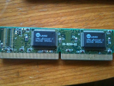
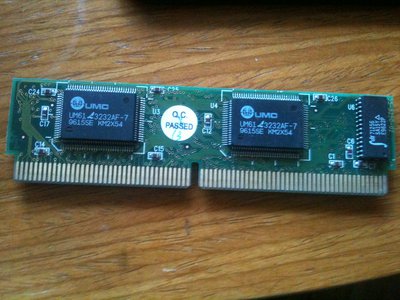
Think I might have found the cache module for your first board last week, came in a bag of random ram sticks i got along with a load of other old bits last weekend.
file.php?mode=view&id=17671&sid=1d7aaf1d3d2bff2c56fe23c66e79e035
file.php?mode=view&id=17670&sid=1d7aaf1d3d2bff2c56fe23c66e79e035

I'm sure someone on here will no whether or not this is the correct part, I dob't have any 486 systems to test or even make an educated guess, but it sure looks like it might be the part!
If it turns out to be the case feel free to PM me, it's of no use to me!
Best regards,
Chris

Attachments

  • cache stick 003.jpg
    Filename
    cache stick 003.jpg
    File size
    1.47 MiB
    Views
    2519 views
    File license
    Fair use/fair dealing exception
  • cache stick 001.jpg
    Filename
    cache stick 001.jpg
    File size
    1.45 MiB
    Views
    2519 views
    File license
    Fair use/fair dealing exception

286 20MHz,1MB RAM,Trident 8900B 1MB, Conner CFA-170A.SB 1350B
386SX 33MHz,ULSI 387,4MB Ram,OAK OTI077 1MB. Seagate ST1144A, MS WSS audio
Amstrad PC 9486i, DX/2 66, 16 MB RAM, Cirrus SVGA,Win 95,SB 16
Cyrix MII 333,128MB,SiS 6326 H0 rev,ESS 1869,Win ME

Reply 14 of 37, by vetz

User metadata
Rank l33t
Rank
l33t
BSA Starfire wrote:

Think I might have found the cache module for your first board last week, came in a bag of random ram sticks i got along with a load of other old bits last weekend.

To me that looks like a regular 512kb PB cache for Socket 7 boards.

3D Accelerated Games List (Proprietary APIs - No 3DFX/Direct3D)
3D Acceleration Comparison Episodes

Reply 15 of 37, by FGB

User metadata
Rank Oldbie
Rank
Oldbie

vetz is right. Sliderider is also right.

This coast stick will FRY your PSU and / or your M919. This coast stick is just PIN-compatible but not electrically compatible with the M919.

NO NOT USE any Pipelined Burst COAST stick with the M919.

@turboman: As said before, the cache on the M912 board is fine, it is just labeled wrong. Some kind of 90s fraud.. Fake cache and wrong labels... nothing to bother. Be happy it's real cache and don't care about the missing 128K.

@sliderider: There is a rare variation of the M919 board which uses DIP-cache instead of the asych cache stick. Very rare though.

www.AmoRetro.de Visit my huge hardware gallery with many historic items from 16MHz 286 to 1000MHz Slot A. Includes more than 80 soundcards and a growing Wavetable Recording section with more than 300 recordings.

Reply 16 of 37, by buyerninety

User metadata
Rank Newbie
Rank
Newbie

FGB said; "..real cache but wrong labels. They are labeled 256K*8
but are infact 128K*8 = 128KB in total.."
I'd disagree with the above sentence as a statement of bald fact -
if you view the jumpering information in the manual for the M912
(which FGB has said that board is), the setting of the jumpers on
the mobo appear to be permanently set for '128KB of L2' .
Therefore, it cannot be factually stated that labels of the (L2)
cache TM TE11256 chips are incorrect.
CACHE MEMORY JUMPER CONFIGURATIONS
================================================
Type...Cache...JP5...JP10....JP11.....JP12......JP13.....JP14
----------------------------------------------------------------
..A.......64K....2-3....2-3....OPEN....OPEN.....OPEN.....OPEN
..B.....128K.....1-2....1-2....OPEN....OPEN.....OPEN.....SHORT
..C.....256K.....2-3....2-3....OPEN....OPEN.....SHORT...SHORT
..D.....256K.....1-2....1-2....OPEN....OPEN.....SHORT...SHORT
....................3-4
..E.....512K.....2-3....2-3....OPEN....SHORT....SHORT...SHORT
....................4-5
..F.....512K.....1-2....1-2....OPEN....SHORT....SHORT...SHORT
....................3-4
....................5-6
..G...1024K.....2-3.....2-3....SHORT...SHORT....SHORT...SHORT
....................4-5
....................6-7
Therefore suggestion by HighTreason" as to "misconfiguration"
may be correct, although it is also possible an OEM reseller did
that to 'limit returns due to misconfigurations by buyers'.
(Also defer to other boardmembers knowledge - is greater than
128Kb L2 going to be significantly more useful, if there is only
8Kb L1 in the CPU??)

Unfortunately, as data for the Tm TE11256 cache chips seem to
be nowhere findable, it is unsure if those chips are internally
32Kx8 or 64Kx8. This has relevence in regard to cache configuration.
CACHE MEMORY CONFIGURATIONS
===============================================
Type....Total Cache....Bank 0.......Bank 1......TAG Ram..Pieces
............................(U21-24)....(.U28-31)....(U20)
---------------------------------------------------------------
..A.........64K...........8K x 8........8K x 8......8K X 8......9
..B........128K..........32K x 8.....................8K X 8......5
..C........256K..........32K x 8......32K x 8.....32K X 8.....9
..D........256K..........64K x 8....................32K X 8......5
..E........512K..........64K x 8......64K x 8.....32K X 8.....9
..F........512K.........128K x 8....................32K X 8......5
..G......1024K.........128K x 8.....128K X 8....64K X 8.....9
Also, the OP may not have tried variations on the bios settings;
Cache Read Hit Wait State, Cache Write Hit Wait State,
DRAM Wait State Select, Alt Bit in Tag SRAM,
which may be having some affect.

Last edited by buyerninety on 2015-04-27, 15:47. Edited 1 time in total.

Reply 17 of 37, by FGB

User metadata
Rank Oldbie
Rank
Oldbie

I've seen at least 10 M912 boards, maybe 15. They come in different configurations. Some with fake chips soldered onto the board, some with mislabeled DIP modules and some with socketed DIP chips. All soldered options had hardwired cache jumpers - only the socketed versions have regular jumpers.
I had some boards with the exact "problem" that the chips indicate 256KB of cache but the jumpers were hardwired for 128KB. I reconfigured these to 256KB but the board failed to work properly, cachechk didn't recognize 256K. Therefore my above statement is not a statement of bald fact but an educated guess and logical assumption. However, I didn't desolder the DIP modules - wasn't worth the effort for me.

Btw: There is no correlation of the L1 cache size of the CPU (depending of which CPU one uses .. goes from 2KB up to 16KB L1 cache) with the onboard L2 cache size. The L2 cache is no command buffer but a buffer for the RAM.
And although different BIOS settings affect the cache speed and some also affect the cacheable memory area, they won't affect the cache size.

www.AmoRetro.de Visit my huge hardware gallery with many historic items from 16MHz 286 to 1000MHz Slot A. Includes more than 80 soundcards and a growing Wavetable Recording section with more than 300 recordings.

Reply 18 of 37, by Sutekh94

User metadata
Rank Oldbie
Rank
Oldbie

Just a few examples of the many different variations of the M912:

M912 with socketed cache
Ditto, different revision (closer to what the OP has)
M912 with soldered cache, exactly the same as the chips on the OP's board

OP seems to have a v1.4 M912 with soldered cache.

That one vintage computer enthusiast brony.
My YouTube | My DeviantArt

Reply 19 of 37, by buyerninety

User metadata
Rank Newbie
Rank
Newbie

FGB, Your experience is helpful, in that it gives clues as to which
lines of investigation are worth following up.
So, from your experience & Turbomans pics, specifically;
http://s636.photobucket.com/user/gijoe25th/me … C07851.jpg.html
I deduce that the ENTIRE bank 1 (U28-31) is populated by
FAKE cache chips, evidenced by the laughable printing (looks
as if a rubber stamp were poorly applied), the solid plastic (no
circular stamp marks which should be present if the chip had
base and top joined to enclose actual 'silicon' chip inside) and
their general poor finish compared to the real cache chips
present in bank 0.
Regarding chips TM TE 11256; there is findable a TM manufacturer,
(actually 'TM Tech' , {they put 'TECH' word on two lines}) which is
'Taiwan Memory Technology Incorporated'. Although I found no
webpage datasheet for that specific chip designation (WaybackMachine
included), and so can't state factually that that is an actual designation,
I believe it is likely to be so, as TM company reports from circa early 90's
cite revenue from product SRAM 256K, further said to be 32Kx8
(and no reference could be found as to any 64Kx8 SRAM chips, even to
year 2000; http://web.archive.org/web/20000407053327/htt … .tw/product.htm ).
(Also, in present day, their SRAM line is only 32Kx8.)

Your wording seemed to indicate to me that you had deduced that
all the 256K chips were wrongly labelled, as maximum of only 128KB
is all you have been able to get through experimentation with the
applicable jumpers. (In regard to the OP's apparently V1.4 board, at
least) how about this possiblity: we should see this;
Total Cache......Bank 0.......Bank 1......TAG Ram..Pieces
...................(U21-24).....(.U28-31)....(U20)
.......256K.......32Kx8........32Kx8.......32Kx8.....9
but because bank 1 is entirely fake chips, what we are getting is this;
½ of 256Kreal..32Kx8real....fake.........32Kx8.....5 actually real chips
because all the bank 1 chips are fake.
Wouldn't four real 256K (labelled) chips (ie, only in bank 0), also give your
observed results of 128KB L2?
Turboman - 'tweren't such a 'Big Mistake', I'm sure others reading this
wish they had your boards... 😀
(especially as then we could test if traces to bank 1 are real, and
if the 'fake chip' pins have no continuity to other pins inside the fake
chip, could easily solder four 256K chips onto the top of the fake
chips, and test {with appropriate changes to the jumpering} if L2
capacity of 256KB is achieveable.)