VOGONS


Reply 720 of 1199, by feipoa

User metadata
Rank l33t++
Rank
l33t++

Sphere:
galanopu's interposer isn't built yet. A common tactic used in marketing is to advertise before its available in order to build anticipation. Yes, I think everyone would like to see how the performance of a board from a "professional PCB designer" stands up to our rag-shag model.

Yes, we should bring back the Cout and Cin pads to the centre, but make them for size 1210.

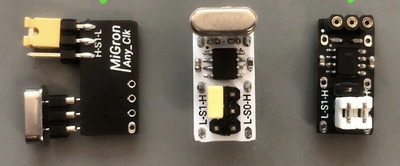
I think no need to make Cin1 2312 and 1210 compatible. Even the MIC had a slightly better output with ceramic placed there. Just make it 1210, or if you need more space 1206. But if you make it 1206, then assembler will be using two different caps for centre region and Cin1, thus this is why I picked 1210. you see 1206 in my images because that is all I had on hand. Also, shrinking Cin1 to 1210 may give you the extra clearance you need for that little stop near the trimmer.

I think looking at the back side of the trimmer would be hideous. I wouldn't flip it at any cost. If wanting to save space further, perhaps we can use a smaller tantalum at Cout? However, ESR will probably increase and I don't know how LP will perform in that case.

If at all possible, it might be best if you swapped the location of the R1 + R2 combination with that of the header. Normally you want the voltage set circuit near Vout, but here we have that part of the circuit on the other side of the the board. Not a big deal if it cannot be flipped because I've already tested it and it is functional as is.

Were you able to implement those PGA solder pads like rasz_pl suggested?

I'm not sure how wide the PCB is at present, but the width of the slim PGA-168 sockets I am using is 1.700". I wouldn't go less than that - not enough PCB real-estate securing the through-holes.

Plan your life wisely, you'll be dead before you know it.

Reply 721 of 1199, by Sphere478

User metadata
Rank l33t++
Rank
l33t++

I meant flipping the way it’s wired haha. You can install it exactly the same way that you did already It is staying exactly as is.You don’t even need to flip it I already flipped the way it is wired up.

Two to vcc one to voltage sense or whatever it is called.

It’s a variable resistor. It should be giving variable resistance no matter this way or the other way. This way the screw turns the oposite way for increase/decrease.

Darn, I was kind of hoping that we had ditched the center region so I could keep all that ground flood oh but, this does give me an excuse to try and figure out away to get back some conductivity to the bottom section that we lost when I pulld the edges back

What is the minimum and number of capacitors in the center? I might be able to fit one under the overhang by the way

I get that he upset you and this is your thread but this thread is really long now and everyone is participating the guys post while lacking a little tact was on topic he is right the responses have been rather toxic to him and I want that to stop

Last edited by Sphere478 on 2022-12-08, 13:22. Edited 3 times in total.

Sphere's PCB projects.
-
Sphere’s socket 5/7 cpu collection.
-
SUCCESSFUL K6-2+ to K6-3+ Full Cache Enable Mod
-
Tyan S1564S to S1564D single to dual processor conversion (also s1563 and s1562)

Reply 722 of 1199, by rasz_pl

User metadata
Rank l33t
Rank
l33t
Sphere478 wrote on 2022-12-08, 06:31:

back 3d - pcb.png

floating unconnected island of copper in the middle, afaik big no no
I dont know about clearances under CPU, is it ok to put components in the middle bottom part? I looked at few pictures of 386 boards and all seemed to have empty space in the socket with no components, feipoa will know better
if yes and you could somehow route 3V there from the top this would be a good spot for two additional 3V cap pads (but 3V must be routed from the top or ideally 3-4 sides, not from bottom)

feipoa wrote on 2022-12-08, 08:52:

Also, shrinking Cin1 to 1210 may give you the extra clearance you need for that little stop near the trimmer.

if things cant be shifted to the left then maybe R1 can overhang the pcb, that notch does look cute 😀 but afaik weird shapes add extra milling/routing charge?

feipoa wrote on 2022-12-08, 08:52:

I'm not sure how wide the PCB is at present, but the width of the slim PGA-168 sockets I am using is 1.700". I wouldn't go less than that - not enough PCB real-estate securing the through-holes.

it does look to be exactly 1.7 weird units wide

Open Source AT&T Globalyst/NCR/FIC 486-GAC-2 proprietary Cache Module reproduction

Reply 723 of 1199, by Sphere478

User metadata
Rank l33t++
Rank
l33t++
rasz_pl wrote on 2022-12-08, 13:21:
floating unconnected island of copper in the middle, afaik big no no I dont know about clearances under CPU, is it ok to put com […]
Show full quote
Sphere478 wrote on 2022-12-08, 06:31:

back 3d - pcb.png

floating unconnected island of copper in the middle, afaik big no no
I dont know about clearances under CPU, is it ok to put components in the middle bottom part? I looked at few pictures of 386 boards and all seemed to have empty space in the socket with no components, feipoa will know better
if yes and you could somehow route 3V there from the top this would be a good spot for two additional 3V cap pads (but 3V must be routed from the top or ideally 3-4 sides, not from bottom)

feipoa wrote on 2022-12-08, 08:52:

Also, shrinking Cin1 to 1210 may give you the extra clearance you need for that little stop near the trimmer.

if things cant be shifted to the left then maybe R1 can overhang the pcb, that notch does look cute 😀 but afaik weird shapes add extra milling/routing charge?

feipoa wrote on 2022-12-08, 08:52:

I'm not sure how wide the PCB is at present, but the width of the slim PGA-168 sockets I am using is 1.700". I wouldn't go less than that - not enough PCB real-estate securing the through-holes.

it does look to be exactly 1.7 weird units wide

The center islands are tying the internal ground planes together

No extra charge for shape

In theory we might be able to put components above and below.

I actually think that maybe we should in fact do this for routing reasons If indeed we are bringing back in the center section I know it won’t be as visually appealing but it will be better but let me look at it

Switching that tantalum to the aforementioned ceramic for CIn may Make just enough space for returning the board to a rectangle But I think we should do what makes the most sense electrically not visually

Sphere's PCB projects.
-
Sphere’s socket 5/7 cpu collection.
-
SUCCESSFUL K6-2+ to K6-3+ Full Cache Enable Mod
-
Tyan S1564S to S1564D single to dual processor conversion (also s1563 and s1562)

Reply 724 of 1199, by Sphere478

User metadata
Rank l33t++
Rank
l33t++

I am trying to figure out a way by the way to make the custom pad shape only on the top layer I was thinking manually using Solder mask and zones what do you all think?

Sphere's PCB projects.
-
Sphere’s socket 5/7 cpu collection.
-
SUCCESSFUL K6-2+ to K6-3+ Full Cache Enable Mod
-
Tyan S1564S to S1564D single to dual processor conversion (also s1563 and s1562)

Reply 725 of 1199, by galanopu

User metadata
Rank Newbie
Rank
Newbie

feipoa: As I said... I can give advice, but not with this attitude. I would always try to reply to polite request if possible.
Saying... "We welcome the critique, not the ego", or again that I am here for marketing or putting "professional PCB designer" in quotes does not help.
I have a day job too, I am super busy and YES I am doing PCB design as a profession for years now.

Now, I was thinking that I will finish testing my design this weekend, however I figured out that I do not have 168p sockets 😒
So I just ordered some. I have individual socket pin headers, but I will probably just wait two weeks for the sockets.
The schematic is nothing special really. I just followed the datasheet, probably very similar your design.
There not many ways to connect in schematic level this actually 132p to 168p.

Now regarding your design here. The main problem is signal integrity, return paths, and cross talk.
All these are impossible to be solved the correct way here!
And the fundamental problem is using JLCs 6-layer stack-up for this complex in place design.
So the problem starts form the initial design decisions.
I also tried to design this in place, 6 Layers.
I concluded it is impossible to do correctly! Especially with JLCs stack-up!
This ether needs a very tweaked and expensive 6L stack-up, or most likely 8 Layers.
I am a bit amazed that this worked that well actually, congrats for the results!

Now to my understating you have not shared Cad or Gerber files, only pictures of the layers so it is hard to tell.
I am not even sure if you have a single solid GND plane there.
Either-way the only thing you can do to improve the situation is to add as many GND vias as possible.
All this GND metal fills should be connected to as many points as possible.
Floating islands or parts connected only on the one side are very bad.
Try also to NOT have lines running in parallel on two different next to each other layers.
And maybe space out some signals on the same layer.

BTW JLC has promo now until end of the year only 20$ for 6 layers, now it is your chance to reorder.
That is for now. ^^

Let's mod everything! Check my youtube channel:
https://www.youtube.com/channel/UCZ6ULBqIKhxuNslAbqFNJUg
Interested in my devices? Check my store:
https://migronelectronics.bigcartel.com

Reply 726 of 1199, by rasz_pl

User metadata
Rank l33t
Rank
l33t
Sphere478 wrote on 2022-12-08, 13:25:

The center islands are tying the internal ground planes together

now I see the via, /slaps forehead sorry

Sphere478 wrote on 2022-12-08, 13:43:

I am trying to figure out a way by the way to make the custom pad shape only on the top layer I was thinking manually using Solder mask and zones what do you all think?

change pad type from thru hole to SMD, put normal thru hole pad on top

galanopu wrote on 2022-12-08, 13:57:

feipoa: As I said... I can give advice, but not with this attitude. I would always try to reply to polite request if possible.
Saying... "We welcome the critique, not the ego", or again that I am here for marketing or putting "professional PCB designer" in quotes does not help.

You posted picture with information you will be selling this, feipoa wasnt thrilled with straight up "look at what you could buy" post, it goes downhill from there with you accusing him of toxicity and shitting on working design. This is a weird drama. 😒

galanopu wrote on 2022-12-08, 13:57:

Now regarding your design here. The main problem is signal integrity, return paths, and cross talk.
All these are impossible to be solved the correct way here!

you would think so, but it works just fine 😀

galanopu wrote on 2022-12-08, 13:57:

Now to my understating you have not shared Cad or Gerber files

because you wouldnt? 😜 they are right here in this thread, multiple versions

galanopu wrote on 2022-12-08, 13:57:

I am not even sure if you have a single solid GND plane there.

nope, all layers are partially flood filled stitched together grounds.

galanopu wrote on 2022-12-08, 13:57:

Try also to NOT have lines running in parallel on two different next to each other layers.

this would be the only mayor issue with currently working one, layer 1 should be swapped with layer 2

galanopu wrote on 2022-12-08, 13:57:

BTW JLC has promo now until end of the year only 20$ for 6 layers, now it is your chance to reorder.
That is for now. ^^

https://jlcpcb.com/help/newsdetail/42-6-Layer … on-PCBs-for-$20

>6-layer, there's a $2 limited-time special offer before 5th January 2023, that the board within 5cm*5cm (5pcs with ENIG and via-in-pad) will be reduced from over $100 to a special price of $2.

this is < 5x5 cm so $2 for five 6 layer, sounds like its time to go wild with different design experiments 😀

Open Source AT&T Globalyst/NCR/FIC 486-GAC-2 proprietary Cache Module reproduction

Reply 727 of 1199, by Sphere478

User metadata
Rank l33t++
Rank
l33t++

Honestly, yes. This interposer working as well as it does AND being this small, is a miracle. It’s like trying to wire up a bowl of spaghetti. Lol

I really wish 8 layer was an option. I would spread these traces out a little farther and put more ground in. It would let me do better power planes also. But 6 layer is working. We sacrificed a little conductive cross section making it smaller. And a couple traces that were straight through are now on vias as they transit. But all in all it looks like it will work.

I’ll upload the latest files soon.

It’s not ready for release yet, but I’ll upload as a progress saver. And for you all to look

You are correct, the full ground plane is only realized by stitching the partial planes from all layers together.

Some traces are grouped trying to improve ground plane.

Like you said, doing this properly was never an option. We give somewhere and it takes somewhere else. I’m stitching it together as good as I can. It seems to have worked! :p

I’ll look into the layer swap

Last edited by Sphere478 on 2022-12-08, 15:15. Edited 3 times in total.

Sphere's PCB projects.
-
Sphere’s socket 5/7 cpu collection.
-
SUCCESSFUL K6-2+ to K6-3+ Full Cache Enable Mod
-
Tyan S1564S to S1564D single to dual processor conversion (also s1563 and s1562)

Reply 728 of 1199, by galanopu

User metadata
Rank Newbie
Rank
Newbie

My initial post was really just presenting pics of my work and saying that I will give updates later.
All my stuff are commercial. This was not a sale speech as this is not even ready.
Normally I only post only when something is ready, and I have a video on that.
I just wanted to inform that I have something, and I will give early results here.

So rasz_pl, ok weird drama, but why you try to attack also here?
I really did NOT shit on a working design!

Telling the truth is not shitting. He also asked me "why no feedback on his design".
Anyone with experience can tell how problematic the routing is here.
And I actually avoided commenting on the design for long to avoid confrontation.
Working is also a relative thing. This should normally work 50MHz on default voltage.
Still quite impressive results given the design, congrats!

Also I never asked for files, I do not care, but I can not give tips by only looking at random screenshots.
At least one solid ground is a must, but looks like that this is also very hard at 6L.
Normally at least 2 GND planes are needed, and all signals should reference one.
And then also a carefully selected stack-up. Just 6L, 8L, 10L means nothing.
So yeah probably 8 Layers for this is minimum. This is not shit talking, I hope you understand.

Let's mod everything! Check my youtube channel:
https://www.youtube.com/channel/UCZ6ULBqIKhxuNslAbqFNJUg
Interested in my devices? Check my store:
https://migronelectronics.bigcartel.com

Reply 729 of 1199, by galanopu

User metadata
Rank Newbie
Rank
Newbie
Sphere478 wrote on 2022-12-08, 15:07:
Honestly, yes. This interposer working as well as it does AND being this small, is a miracle. It’s like trying to wire up a bowl […]
Show full quote

Honestly, yes. This interposer working as well as it does AND being this small, is a miracle. It’s like trying to wire up a bowl of spaghetti. Lol

I really wish 8 layer was an option. I would spread these traces out a little farther and put more ground in. It would let me do better power planes also. But 6 layer is working. We sacrificed a little conductive cross section making it smaller. And a couple traces that were straight through are now on vias as they transit. But all in all it looks like it will work.

I’ll upload the latest files soon.

It’s not ready for release yet, but I’ll upload as a progress saver. And for you all to look

You are correct, the full ground plane is only realized by stitching the partial planes from all layers together.

Some traces are grouped trying to improve ground plane.

Like you said, doing this properly was never an option. We give somewhere and it takes somewhere else. I’m stitching it together as good as I can. It seems to have worked! :p

I’ll look into the layer swap

All true 😀
I might have a look when you give files. If I see something very bad and fixable I will tell.
BTW, My design is 4L. Everything is routed more or less the good way.
I am very hopeful, we will see... I also have 486sxl2-G66 cpus.
And for sure modded M/Bs that can do any bus speed up to 55.

Let's mod everything! Check my youtube channel:
https://www.youtube.com/channel/UCZ6ULBqIKhxuNslAbqFNJUg
Interested in my devices? Check my store:
https://migronelectronics.bigcartel.com

Reply 730 of 1199, by maxtherabbit

User metadata
Rank l33t
Rank
l33t

coming into a thread about a community designed open source device with a closed source commercial pay to play "alternative" is just a bad look, I'm shocked you don't understand that

more likely you do and just don't care

Reply 731 of 1199, by galanopu

User metadata
Rank Newbie
Rank
Newbie

My thinking was, that it is pointless to do multiple threads on the same topic 486SXL2 132p to 168p.
OK, If the creator of the thread "feipoa" does not like to see my results, in the end I go do an other thread,
and maybe delete all my comments here and also stop helping here, depends on his will in the end.
Commercial and open can coexist in my mind. Just more options.

Let's mod everything! Check my youtube channel:
https://www.youtube.com/channel/UCZ6ULBqIKhxuNslAbqFNJUg
Interested in my devices? Check my store:
https://migronelectronics.bigcartel.com

Reply 732 of 1199, by rasz_pl

User metadata
Rank l33t
Rank
l33t
galanopu wrote on 2022-12-08, 15:10:

I really did NOT shit on a working design!

>Believe me, you do not want to hear my critique on the design choices here.

Does sounds like a threat.

galanopu wrote on 2022-12-08, 15:10:

Telling the truth is not shitting.

Thats a very on the spectrum point of view.
"I am not that social to work with others" explains the miscommunication. Probably half of us here have at least moments like that.

galanopu wrote on 2022-12-08, 15:10:

And I actually avoided commenting on the design for long to avoid confrontation.

From the outside this looks as "Mine is going to be the good one. No point helping those guys, but ill advertise here anyway. Oh no, Im shocked they didnt like my advert for commercial product and are attacking me".
Its a lot easier to sympathize with side doing open source design.

galanopu wrote on 2022-12-08, 15:10:

Working is also a relative thing. This should normally work 50MHz on default voltage.

Are you saying yours guarantees it? Fantastic!

galanopu wrote on 2022-12-08, 15:10:

Normally at least 2 GND planes are needed

Werent most 386 boards 4 layer? Yes, shoving full ground plane between every signal layers would be by the book, but we arent manufacturing modern graphic cards here. People did 2 layer 386SX dev boards back in the day.

Open Source AT&T Globalyst/NCR/FIC 486-GAC-2 proprietary Cache Module reproduction

Reply 733 of 1199, by maxtherabbit

User metadata
Rank l33t
Rank
l33t
Sphere478 wrote on 2022-12-08, 12:56:

I get that he upset you and this is your thread but this thread is really long now and everyone is participating the guys post while lacking a little tact was on topic he is right the responses have been rather toxic to him and I want that to stop

The responses he's getting are perfectly commensurate with his attitude and comportment

Reply 734 of 1199, by Sphere478

User metadata
Rank l33t++
Rank
l33t++

Everyone, do me a favor. Please say sorry wether you think you are wrong or not and let us get back to topic. I personally would love to hear about his device and think that it fits in this thread. Perhaps not as an ad, but as a talking point and q&a on design.

Feiopa, what are you using for the overclocking?

I was thinking of getting one or two of these.

Seems handy for fine tuning.

Attachments

Sphere's PCB projects.
-
Sphere’s socket 5/7 cpu collection.
-
SUCCESSFUL K6-2+ to K6-3+ Full Cache Enable Mod
-
Tyan S1564S to S1564D single to dual processor conversion (also s1563 and s1562)

Reply 735 of 1199, by galanopu

User metadata
Rank Newbie
Rank
Newbie

This is exactly what I wanted to avoid, confrontation in some forum. You two are proving my point.
I will not answer anymore to attacks. People are not interested reading other fighting.
Lets keep the destitution in topic and to the technical stuff. What I will do next only depends on feipoa's will.

To the technical point, 386DX 486SXL or not if you want to do this in place with 6L and no GND is just bad.
This is just the technical truth, nothing else.

Let's mod everything! Check my youtube channel:
https://www.youtube.com/channel/UCZ6ULBqIKhxuNslAbqFNJUg
Interested in my devices? Check my store:
https://migronelectronics.bigcartel.com

Reply 736 of 1199, by Sphere478

User metadata
Rank l33t++
Rank
l33t++

I will have a very brief period in a few hours to work on this and upload. Then possibly not again for a while. Anything that needs done based on pics?

How many caps do you want in center? 1210 size in center? Are we changing cin to 1210? (I may be remembering wrong size number)

I wanna try and figure out how to make those vias only shaped like that on one layer so I can put internal traces back where they were before. So I’ll work on that.

Sphere's PCB projects.
-
Sphere’s socket 5/7 cpu collection.
-
SUCCESSFUL K6-2+ to K6-3+ Full Cache Enable Mod
-
Tyan S1564S to S1564D single to dual processor conversion (also s1563 and s1562)

Reply 737 of 1199, by galanopu

User metadata
Rank Newbie
Rank
Newbie

OK, in the end I could not wait for a socket... I soldered a G66 directly into the adapter.
It worked on the first try 100% stable at 2 x 33.3 = 66.6 MHz with 3.3V. Cache enabled.
Now in some benchmarks it is actuality slower than my 486DLC @ 55MHz!
In general... Integer tests are faster and Floating slower. Yeah... bus limited.
However ok, it is OC time now. 😀
I can control vcore up to 4.1v with 0.1v steps.
These is also some tweaking to do here. I will just make a video with the OC tweaked results.

Edit: This can also do 1x 55MHz in the end, I just had to increase the vcore to 3.6V.

Attachments

  • IMG_1691.JPG
    Filename
    IMG_1691.JPG
    File size
    87.83 KiB
    Views
    776 views
    File license
    Public domain
  • IMG_1689.JPG
    Filename
    IMG_1689.JPG
    File size
    754.99 KiB
    Views
    776 views
    File license
    Public domain
  • IMG_1688.JPG
    Filename
    IMG_1688.JPG
    File size
    172.39 KiB
    Views
    776 views
    File license
    Public domain
  • IMG_1685.JPG
    Filename
    IMG_1685.JPG
    File size
    356.42 KiB
    Views
    776 views
    File license
    Public domain
  • IMG_1684.JPG
    Filename
    IMG_1684.JPG
    File size
    224.46 KiB
    Views
    776 views
    File license
    Public domain
Last edited by galanopu on 2022-12-09, 01:27. Edited 1 time in total.

Let's mod everything! Check my youtube channel:
https://www.youtube.com/channel/UCZ6ULBqIKhxuNslAbqFNJUg
Interested in my devices? Check my store:
https://migronelectronics.bigcartel.com

Reply 738 of 1199, by Sphere478

User metadata
Rank l33t++
Rank
l33t++

Very nice 😀 I see you soldered all of the vcc pins you could get to with capacitors. What value did you use? What does your power plane look like on the oscilloscope?

What do the parts in the middle do?

Sphere's PCB projects.
-
Sphere’s socket 5/7 cpu collection.
-
SUCCESSFUL K6-2+ to K6-3+ Full Cache Enable Mod
-
Tyan S1564S to S1564D single to dual processor conversion (also s1563 and s1562)

Reply 739 of 1199, by galanopu

User metadata
Rank Newbie
Rank
Newbie
Sphere478 wrote on 2022-12-09, 01:23:

Very nice 😀 I see you soldered all of the vcc pins you could get to with capacitors.

Yes this was by design. It is a good idea that you will do that also.

Sphere478 wrote on 2022-12-09, 01:23:

What value did you use?

10u, a very classic thing that I have done also to my 386 / 486 M/Bs
https://youtu.be/eUaoXPgnZvo?t=780

Sphere478 wrote on 2022-12-09, 01:23:

What does your power plane look like on the oscilloscope?

No reason to measure. I know by design that this is more than enough.
As said, this works at 66Mhz 3.3V, and I am actually running now at 80MHz no problem.
Maybe I hit 100MHz in the end, we will see.

You should be careful with the oscilloscope, it is very easy to record irrelevant noise.
iIdealy you should remove the alligator ground wire and use a special ground spring, if you have.
The longer the gnd connection and the further apart the more noise you will see incorrectly!
https://electronics.stackexchange.com/questio … e-ground-spring

BTW I do not have a Power plane. A proper GND plane is way more important.

Sphere478 wrote on 2022-12-09, 01:23:

What do the parts in the middle do?

Just decoupling and the vreg control. Also controlling the KEN input, you can check this again on my video:
https://youtu.be/KDQsLDN9df8?t=807

Let's mod everything! Check my youtube channel:
https://www.youtube.com/channel/UCZ6ULBqIKhxuNslAbqFNJUg
Interested in my devices? Check my store:
https://migronelectronics.bigcartel.com