VOGONS


Reply 480 of 1186, by feipoa

User metadata
Rank l33t++
Rank
l33t++
elbbar wrote on 2022-11-12, 15:27:

I would suggest adding several bypass capacitors near the CPU.

Are you referring to adding bypass capacitors to the voltage set resistor(s) or adding more decoupling capacitors? In either case, could you be more specific with which capacitor values should be used and where?

Plan your life wisely, you'll be dead before you know it.

Reply 481 of 1186, by elbbar

User metadata
Rank Newbie
Rank
Newbie

Food for thought.

https://invidious.snopyta.org/watch?v=KDQsLDN9df8
https://invidious.snopyta.org/watch?v=1xicZF9glH0
https://invidious.snopyta.org/watch?v=BcJ6UdDx1vg

bypass.jpg
Filename
bypass.jpg
File size
169.53 KiB
Views
1035 views
File license
CC-BY-4.0

Reply 482 of 1186, by feipoa

User metadata
Rank l33t++
Rank
l33t++

elbbar, I'm not sure what you are showing a photo of, but it doesn't look like a 386 or 486 interposer. Our later designs have a total of 10 capacitor pads for Vin and Vout. Could you be more specific with what you are recommending? All I can think of is adding bypass capacitor in parallel to to the voltage setting resistor, R2. When I looked into this some months ago, I decided it probably wasn't necessary, but it is easy enough to test on the beta.

SXL2_interposer_soldering_order_3.JPG
Filename
SXL2_interposer_soldering_order_3.JPG
File size
158.98 KiB
Views
1014 views
File license
CC-BY-4.0

Plan your life wisely, you'll be dead before you know it.

Reply 483 of 1186, by Sphere478

User metadata
Rank l33t++
Rank
l33t++

Ti 486SXL2-50 on some kind of adapter... what is this for?

Cross linking

Sphere's PCB projects.
-
Sphere’s socket 5/7 cpu collection.
-
SUCCESSFUL K6-2+ to K6-3+ Full Cache Enable Mod
-
Tyan S1564S to S1564D single to dual processor conversion (also s1563 and s1562)

Reply 484 of 1186, by feipoa

User metadata
Rank l33t++
Rank
l33t++

In the start of that thread, that adapter is on a PGA132 CPU. It helps with cache coherency issues on some obscure systems. Evergreen made one, as did Kingston. I found that none of the 8 or so 386 motherboards I tested needed this adapter. Later in the thread, there's another adaptor for a PGA168 Cyrix 486. That 486 is nothing like the SXL2 PGA168 CPU made by TI. All that later adaptor does is let you run an FPU on that early Cyrix 486 because it didn't have an onboard CPU in the die.

Plan your life wisely, you'll be dead before you know it.

Reply 485 of 1186, by rafpereira

User metadata
Rank Newbie
Rank
Newbie
feipoa wrote on 2022-11-20, 00:17:

In the start of that thread, that adapter is on a PGA132 CPU. It helps with cache coherency issues on some obscure systems. Evergreen made one, as did Kingston. I found that none of the 8 or so 386 motherboards I tested needed this adapter. Later in the thread, there's another adaptor for a PGA168 Cyrix 486. That 486 is nothing like the SXL2 PGA168 CPU made by TI. All that later adaptor does is let you run an FPU on that early Cyrix 486 because it didn't have an onboard CPU in the die.


I can't tell you if this was for SXL2, as I did not take those... but I hope the pictures will serve as inspiration.

74VHC00 - https://utcdn.utsource.info/pdfjs/index.html? … HILD_74VHC04MTC
74HC4024D - https://utcdn.utsource.info/pdfjs/index.html? … I_CD54_74HCT374

Attachments

  • front.jpg
    Filename
    front.jpg
    File size
    288.18 KiB
    Views
    940 views
    File license
    Public domain
  • back2.jpg
    Filename
    back2.jpg
    File size
    288.93 KiB
    Views
    940 views
    File license
    Public domain

Reply 486 of 1186, by feipoa

User metadata
Rank l33t++
Rank
l33t++

Thanks. I have this adaptor. It was for a 5 V SXL. We are trying to make this for a 3.6 V CPU. Still waiting for shipment to arrive...

Plan your life wisely, you'll be dead before you know it.

Reply 487 of 1186, by feipoa

User metadata
Rank l33t++
Rank
l33t++

Quick update: the new PCB's are here and all pins go where they are supposed to. Silkscreen over vias seems OK. I didn't check U1 and U2. Is there a diagram showing where these should go?

Scanned it this time:

SXL2_Interposer_second_batch_JLCPCB.jpg
Filename
SXL2_Interposer_second_batch_JLCPCB.jpg
File size
540.46 KiB
Views
895 views
File license
CC-BY-4.0

Plan your life wisely, you'll be dead before you know it.

Reply 488 of 1186, by Sphere478

User metadata
Rank l33t++
Rank
l33t++

They look very good!

I kind of just copied what was done on the other PCB he checked it and said it was OK. for your uses I don’t think you will be using it so simply do not populate it unless you have a board you can test it on

Sphere's PCB projects.
-
Sphere’s socket 5/7 cpu collection.
-
SUCCESSFUL K6-2+ to K6-3+ Full Cache Enable Mod
-
Tyan S1564S to S1564D single to dual processor conversion (also s1563 and s1562)

Reply 489 of 1186, by Sphere478

User metadata
Rank l33t++
Rank
l33t++

Some of those vias look like they don’t have holes… I’m sure they are fine but can you look closer at that? Probably just image quality. Prob fine.

Sphere's PCB projects.
-
Sphere’s socket 5/7 cpu collection.
-
SUCCESSFUL K6-2+ to K6-3+ Full Cache Enable Mod
-
Tyan S1564S to S1564D single to dual processor conversion (also s1563 and s1562)

Reply 490 of 1186, by feipoa

User metadata
Rank l33t++
Rank
l33t++

You mean the vias on the 4 corners and some in the centre region? It's not image quality. The vias aren't obvious. I did check every single pin though.

Plan your life wisely, you'll be dead before you know it.

Reply 491 of 1186, by Sphere478

User metadata
Rank l33t++
Rank
l33t++

Yeah, there are a bunch that just look flat 🤣. I’m sure it’s fine though 😀

Sphere's PCB projects.
-
Sphere’s socket 5/7 cpu collection.
-
SUCCESSFUL K6-2+ to K6-3+ Full Cache Enable Mod
-
Tyan S1564S to S1564D single to dual processor conversion (also s1563 and s1562)

Reply 492 of 1186, by Sphere478

User metadata
Rank l33t++
Rank
l33t++

I’ve been holding my breath waiting for an update. I’m kinda a vogons purple color now. :p had a chance to assemble it?

I’ve been looking closely at the images. I see a few solder blobs under the silk but otherwise everything looks amazing. Can’t wait for you to plug it in and see how high you can clock it!

Sphere's PCB projects.
-
Sphere’s socket 5/7 cpu collection.
-
SUCCESSFUL K6-2+ to K6-3+ Full Cache Enable Mod
-
Tyan S1564S to S1564D single to dual processor conversion (also s1563 and s1562)

Reply 493 of 1186, by feipoa

User metadata
Rank l33t++
Rank
l33t++

I was going to assemble it tonight, but my wife has been getting on my case about staying up late with these self-imposed hobby tasks.

Plan your life wisely, you'll be dead before you know it.

Reply 494 of 1186, by feipoa

User metadata
Rank l33t++
Rank
l33t++

I've soldered on all the PGA pins now, top and bottom. With interruptions, it took 1 hr. 45 min. Without, probably would take 1 hr. The trickiest part would be the inner 4 corners. Don't accidentally get solder in an adjacent empty via, or it can be difficult to get out.

The distance from the PGA168 socket to the edge of the PCB is 1.30 mm. Conservatively, we could probably trim 1 mm off all 4 sides, assuming that 1 mm wide perimeter is imperative for trace real-estate. The header with 5 through-holes can be nudged maybe 0.5 mm to 0.7 mm closer to the socket to help meet the clearance. I wouldn't spend any more time on the layout until we know it works though.

Plan your life wisely, you'll be dead before you know it.

Reply 495 of 1186, by Sphere478

User metadata
Rank l33t++
Rank
l33t++

Do you think making it smaller will actually help on any boards? Are there boards with clearance issues that tight?

I can understand it maybe hitting the fet side, but the sides?

Sphere's PCB projects.
-
Sphere’s socket 5/7 cpu collection.
-
SUCCESSFUL K6-2+ to K6-3+ Full Cache Enable Mod
-
Tyan S1564S to S1564D single to dual processor conversion (also s1563 and s1562)

Reply 496 of 1186, by feipoa

User metadata
Rank l33t++
Rank
l33t++

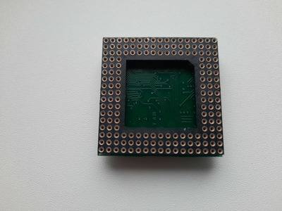
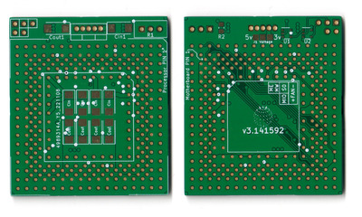
I don't own every 386 motherboard out there, so I cannot say for certain if the reduction by 1 mm will help. I am talking about all 4 sides, not just the FET side. I have on a few occasions had upgrade adapters just barely not fit and it is irritating. I either have to desolder a cap on the motherboard and replace it with a smaller one, bend the cap out of the way, or have to use PGA extension sockets to make the clearance.

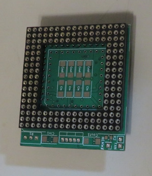
The other adaptor I have, same one that the other poster just provided a photo of, I use it with an additonal VRM module, and on one baord, it just barely hits the reset header on the motherboard. So I had to use an extension socket to make the clearance. In such a case, if it was 1 mm smaller, I wouldn't have to use sockets to lift up the board.

It may only be worth the effort to shrink the board by 1 mm on all 4 sides if something else of greater importance needs to be changed on the design.

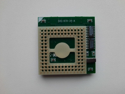
Luckily, the 1210 ceramic capacitors I ordered will fit the existing design, as well the smaller 1411 tantalums. Just barely, but enough that solder won't have to bridge an air gap.

Plan your life wisely, you'll be dead before you know it.

Reply 498 of 1186, by Sphere478

User metadata
Rank l33t++
Rank
l33t++

I looked at the images from
Earlier in thread to refresh myself, (I’m still away from computer) and if you want it smaller, the edge capacitors gotta go.

Or, it will have to be a non rectangular shape.

So options are:

1: Leave as is

2: irregular shape

3: smaller rectangular but ditch the edge caps

I campaigned to remove the edge caps earlier but you wanted to keep them because they look cool. And I agree they do. I’m actually happy we kept them, you were right about them looking cool 🤣
But if you want smaller, they gotta go.

I’m leaning toward leave as is. Doesn’t seem like it’s worth it to alter it at this point.

I have thought up an idea to flip the center caps around 180* though.

To make the path to the regulator more direct. But it isn’t necessary.

Sphere's PCB projects.
-
Sphere’s socket 5/7 cpu collection.
-
SUCCESSFUL K6-2+ to K6-3+ Full Cache Enable Mod
-
Tyan S1564S to S1564D single to dual processor conversion (also s1563 and s1562)

Reply 499 of 1186, by feipoa

User metadata
Rank l33t++
Rank
l33t++

I don't quite follow how the VRM's left/right caps follow shrinking the PCB footprint on the far side of the PCB. Seems unrelated.

It is the giant pin header which is the limiting factor on the overhangs protrusion distance right now, not the side caps.

Normally, primary output for VRM's should be placed as close as possible to the VRM.

I am wondering if the centre input caps serve any purpose. Seems like only the centre output caps serve a purpose.

feipoa wrote on 2022-11-26, 03:03:

I wouldn't spend any more time on the layout until we know it works though.

Plan your life wisely, you'll be dead before you know it.