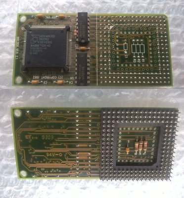
So i found quite a few different control signals from datasheets. I think most of them can be dealt with. I have divided them into 5 groups as follows:
1. 486 specific signal. These are JTAG connections, voltage sence and clock multiplier. I think they can all be ignored in the adaptor.
2. Numeric co-pro controls. I think they can be ignored for now too.
3. Cache controls. I think they can easily be dealt with for the begining by disabling the cache.
4. Cache related signals. I do not understand them all, but they do not seem unsolvable.
5. Bus controls. 486 support parity checks, but these can be disabled. Although 386 has BS16 signal to indicate a 16 bid bus request. 486 has BS16 and BS8 signals. I dunno where we can wire a BS8.
full list of 486 signals not found in 386 datasheet:
Group 1. 486 specific signals. I am quite convinced these may be ignored:
CLKMUL - Clock Multiplier (Input)
The microprocessor samples the CLKMUL input signal at RESET to determine the design operating frequency.
SMI - SMM Interrupt (Active Low; Input)
A Low signal on the SMI pin signals the processor to enter System Management mode (SMM). SMI is the highest level processor interrupt. The SMI signal is recognized on an instruction boundary, similar to the NMI and INTR signals. SMI is sampled on every rising clock edge. SMI is a falling-edge sensitive input. The SMI input has an internal pull-up resister. Recognition of SMI is guaranteed in a specific clock if it is asserted synchronously and meets the setup and hold times. If SMI is asserted asynchronously, it must go High for a minimum of two clocks before going Low, and it must remain Low for at least two clocks to guarantee recognition. When the CPU recognizes SMI, it enters SMM before executing the next instruction and saves internal registers in SMM space.
SMIACT - SMM Interrupt Active (Active Low; Output)
SMIACT goes Low in response to SMI. It indicates that the processor is operating under SMM control. SMIACT remains Low until the processor receives a RESET signal or executes the Resume Instruction (RSM) to leave SMM. This signal is always driven. It does not float during bus HOLD or BOFF.
Note:
Do not use SRESET to exit from SMM. The system should block SRESET during SMM.
SRESET - Soft Reset (Active High; Input)
The CPU samples SRESET on every rising clock edge. If SRESET is sampled active, the SRESET sequence begins on the next instruction boundary. SRESET resets the processor, but, unlike RESET, does not cause it to sample UP or WB/WT, or affect the FPU, cache, CD and NW bits in CR0, and SMBASE. SRESET is asynchronous and must meet the same timing as RESET. The SRESET input has an internal pull-down resistor.
STPCLK - Stop Clock (Active Low; Input)
A Low input signal indicates a request has been made to turn off the CLK input. When the CPU recognizes a STPCLK, the processor:
- Stops execution on the next instruction boundary (unless superseded by a higher priority interrupt)
- Empties all internal pipelines and write buffers
- Generates a Stop Grant acknowledge bus cycle
STPCLK is active Low and has an internal pull-up resistor. STPCLK is asynchronous, but it must meet setup and hold times t20 and t21 to ensure recognition in any specific clock. STPCLK must remain active until the Stop Clock special bus cycle is issued and the system returns either RDY or BRDY.
TCK - Test Clock (Input)
Test Clock provides the clocking function for the JTAG boundary scan feature. TCK clocks state information and data into the component on the rising edge of TCK on TMS and TDI, respectively. Data is clocked out of the component on the falling edge of TCK on TDO. TCK uses an internal weak pull-up.
TDI - Test Data Input (Input)
TDI is the serial input that shifts JTAG instructions and data into the tested component. TDI is sampled on the rising edge of TCK during the SHIFT-IR and the SHIFT-DR TAP (Test Access Port) controller states. During all other TAP controller states, TDI is ignored. TDI uses an internal weak pull-up.
TDO - Test Data Output (Active High; Output)
TDO is the serial output that shifts JTAG instructions and data out of the component. TDO is driven on the falling edge of TCK during the SHIFT-IR and SHIFT-DR TAP controller states. Otherwise, TDO is three-stated.
TMS - Test Mode Select (Active High; Input)
TMS is decoded by the JTAG TAP to select the operation of the test logic. TMS is sampled on the rising edge of TCK. To guarantee deterministic behavior of the TAP controller, the TMS pin has an internal pull-up resistor.
UP - Write/Read (Input)
The processor samples the Upgrade Present (UP) pin in the clock before the falling edge of RESET. If it is Low, the processor three-states its outputs immediately. UP must remain asserted to keep the processor inactive. The pin uses an internal pull-up resistor.
VOLDET (168-Pin PGA Package Only) - Voltage Detect (Output)
VOLDET provides an external signal to allow the system to determine the CPU input power level (3 V or 5 V). For the Enhanced Am486DX microprocessors, the pin ties internally to VSS.
Group 2. Numeric co-processor controls. Can be ignored for start I think:
IGNNE - Ignore Numeric Error (Active Low; Input)
When this pin is asserted, the Enhanced Am486DX microprocessors will ignore a numeric error and continue executing non-control floating-point instructions. When IGNNE is deasserted, the Enhanced Am486DX microprocessors will freeze on a non-control floating-point instruction if a previous floating-point instruction caused an error. IGNNE has no effect when the NE bit in Control Register 0 is set. IGNNE is active Low and is provided with a small internal pullup resistor. IGNNE is asynchronous but must meet setup and hold times t20 and t21 to ensure recognition in any specific clock.
FERR - Floating-Point Error (Active Low; Output)
Driven active when a floating-point error occurs, FERR is similar to the ERROR pin on a 387 math coprocessor. FERR is included for compatibility with systems using DOS-type floating-point error reporting. FERR is active Low, and is not floated during bus hold, except during three-state Test mode (see FLUSH).
Groups 3. Cache. 486 processor can control cache. Here are the control signals, related to cache:
CACHE - Internal Cacheability (Active Low; Output)
In Write-through mode, this signal always floats. In Write-back mode for processor-initiated cycles, a Low output on this pin indicates that the current read cycle is cacheable, or that the current cycle is a burst write-back or copy-back cycle. If the CACHE signal is driven High during a read, the processor will not cache the data even if the KEN pin signal is asserted. If the processor determines that the data is cacheable, CACHE goes active when ADS is asserted and remains in that state until the next RDY or BRDY is asserted. CACHE floats in response to a BOFF or HOLD request.
FLUSH - Cache Flush (Active Low; Input)
In Write-back mode, FLUSH forces the microprocessor to write-back all modified cache lines and invalidate its internal cache. The microprocessor generates two flush acknowledge special bus cycles to indicate completion of the write-back and invalidation. In Write-through mode, FLUSH invalidates the cache without issuing a special bus cycle. FLUSH is an active Low input that needs to be asserted only for one clock. FLUSH is asynchronous, but setup and hold times t20 and t21 must be met for recognition in any specific clock. Sampling FLUSH Low in the clock before the falling edge of RESET causes the microprocessor to enter three-state Test mode.
HITM - Hit Modified Line (Active Low; Output)
In Write-back mode (WB/WT=1 at RESET), HITM indicates that an external snoop cache tag comparison hit a modified line. When a snoop hits a modified line in the internal cache, the microprocessor asserts HITM two clocks after EADS is asserted. The HITM signal stays asserted (Low) until the last BRDY for the corresponding write-back cycle. At all other times, HITM is deasserted (High). During RESET, the HITM signal can be used to detect whether the CPU is operating in Write-back mode. In Write-back mode (WB/WT=1 at RESET), HITM is deasserted(driven High) until the first snoop that hits a modified line. In Write-through mode, HITM floats at all times.
INV - Invalidate (Active High; Input)
The external system asserts INV to invalidate the cache line state when an external bus master proposes a write. It is sampled together with A31–A4 during the clock in which EADS is active. INV has an internal weak pull-up. INV is ignored in Write-through mode.
KEN - Cache Enable (Active Low; Input)
KEN determines whether the current cycle is cacheable. When the microprocessor generates a cacheable cycle and KEN is active one clock before RDY or BRDY during the first transfer of the cycle, the cycle becomes a cache line fill cycle. Returning KEN active one clock before RDY during the last read in the cache line fill causes the line to be placed in the on-chip cache. KEN is active Low and is provided with a small internal pull-up resistor. KEN must satisfy setup and hold times t14 and t15 for proper operation.
WB/WT - Write-Back/Write-Through (Input)
If the processor samples WB/WT High at RESET, the processor is configured in Write-back mode and all subsequent cache line fills sample WB/WT on the same clock edge in which it finds either RDY or the first BRDY of a burst transfer to determine if the cache line is designated as Write-back mode or Write-through. If the signal is Low on the first BRDY or RDY, the cache line is write-through. If the signal is High, the cache line is write-back. If WB/WT is sampled Low at RESET, all cache line fills are write-through. WB/WT has an internal weak pull-down.
These signal can hopefully be ignored if cache is disabled in BIOS (some signals need to be pulled up I think but this is pretty straight forward)
Group 4. Following signals I THINK are related to cache and MAYBE may be ignored. Or not:
PCD - Page Cache Disable (Active High; Output)
This pin reflects the state of the PCD bit in the page table entry or page directory entry (programmable through the PCD bit in CR3). If paging is disabled, the CPU ignores the PCD bit and drives the PCD output Low. PCD has the same timing as the cycle definition pins (M/IO, D/C, and W/R). PCD is active High and is not driven during bus hold. PCD is masked by the Cache Disable bit (CD) in Control Register 0 (CR0).
PLOCK - Pseudo-Lock (Active Low; Output)
In Write-back mode, the processor forces the output High and the signal is always read as inactive. In Write-through mode, PLOCK operates normally. When asserted, PLOCK indicates that the current bus transaction requires more than one bus cycle. Examples of such operations are segment table descriptor reads (8 bytes) and cache line fills (16 bytes). The microprocessor drives PLOCK active until the addresses for the last bus cycle of the transaction have been driven, whether or not RDY or BRDY is returned. PLOCK is a function of the BS8, BS16, and KEN inputs. PLOCK should be sampled on the clock when RDY is returned. PLOCK is active Low and is not driven during bus hold.
A20M - Address Bit 20 Mask (Active Low; Input)
A Low signal on the A20M pin causes the microprocessor to mask address line A20 before performing a look up to the internal cache, or driving a memory cycle on the bus. Asserting A20M causes the processor to wrap the address at 1 Mbyte, emulating Real mode operation. The signal is asynchronous, but must meet setup and hold times t20 and t21 for recognition during a specific clock. During normal operation, A20M should be sampled High at the falling edge of RESET.
PWT - Page Write-Through (Active High; Output)
This pin reflects the state of the PWT bit in the page table entry or page directory entry (programmable through the PWT bit in CR3). If paging is disabled, the CPU ignores the PWT bit and drives the PWT output Low. PWT has the same timing as the cycle definition pins (M/IO, D/C, and W/R). PWT is active High and is not driven during bus hold
RDY - Non-Burst Ready (Active Low; Input)
A Low input on this pin indicates that the current bus cycle is complete, that is, either the external system has presented valid data on the data pins in response to a read, or the external system has accepted data from the microprocessor in response to a write. RDY is ignored when the bus is idle and at the end of the bus cycle’s first clock. RDY is active during address hold. Data can be returned to the processor while AHOLD is active. RDY is active Low and does not have an internal pull-up resistor. RDY must satisfy setup and hold times t16 and t17 for proper chip operation.
BLAST - Burst Last (Active Low; Output)
Burst Last goes Low to tell the CPU that the next BRDY signal completes the burst bus cycle. BLAST is active for both burst and non-burst cycles. BLAST is active Low and is not driven during a bus hold.
BOFF - Back Off (Active Low; Input)
This input signal forces the microprocessor to float all pins normally floated during hold, but HLDA is not asserted in response to BOFF. BOFF has higher priority than RDY or BRDY; if both are returned in the same clock, BOFF takes effect. The microprocessor remains in bus hold until BOFF goes High. If a bus cycle is in progress when BOFF is asserted, the cycle restarts. BOFF must meet setup and hold times t18 and t19 for proper operation. BOFF has an internal weak pull-up.
BRDY - Burst Ready Input (Active Low; Input)
The BRDY signal performs the same function during a burst cycle that RDY performs during a non-burst cycle. BRDY indicates that the external system has presented valid data in response to a read, or that the external system has accepted data in response to a write. BRDY is ignored when the bus is idle and at the end of the first clock in a bus cycle. BRDY is sampled in the second and subsequent clocks of a burst cycle. The data presented on the data bus is strobed into the microprocessor when BRDY is sampled active. If RDY is returned simultaneously with BRDY, BRDY is ignored and the cycle is converted to a non-burst cycle. BRDY is active Low and has a small pull-up resistor, and must satisfy the setup and hold times t16 and t17
BREQ - Internal Cycle Pending (Active High; Output)
BREQ indicates that the microprocessor has generated a bus request internally, whether or not the microprocessor is driving the bus. BREQ is active High and is floated only during three-state Test mode (see FLUSH).
AHOLD - Address Hold (Active High; Input)
The external system may assert AHOLD to perform a cache snoop. In response to the assertion of AHOLD, the microprocessor stops driving the address bus A31–A2 in the next clock. The data bus remains active and data can be transferred for previously issued read or write bus cycles during address hold. AHOLD is recognized even during RESET and LOCK. The earliest that AHOLD can be deasserted is two clock cycles after EADS is asserted to start a cache snoop. If HITM is activated due to a cache snoop, the microprocessor completes the current bus activity and then asserts ADS and drives the address bus while AHOLD is active. This starts the write-back of the modified line that was the target of the snoop.
EADS - External Address Strobe (Active Low; Input)
This signal indicates that a valid external address has been driven on the address pins A31–A4 of the microprocessor to be used for a cache snoop. This signal is recognized while the processor is in hold (HLDA is driven active), while forced off the bus with the BOFF input, or while AHOLD is asserted. The microprocessor ignores EADS at all other times. EADS is not recognized if HITM is active, nor during the clock after ADS, nor during the clock after a valid assertion of EADS. Snoops to the on-chip cache must be completed before another snoop cycle is initiated. Table 3 describes EADS when first sampled. EADS can be asserted every other clock cycle as long as the hold remains active and HITM remains inactive. INV is sampled in the same clock period that EADS is asserted. EADS has an internal weak pull-up.
Group 5. Bus controls
DP3–DP0 - Data Parity (Inputs/Outputs)
Data parity is generated on all write data cycles with the same timing as the data driven by the microprocessor. Even parity information must be driven back into the microprocessor on the data parity pins with the same timing as read information to ensure that the processor uses the correct parity check. The signals read on these pins do not affect program execution. Input signals must meet setup and hold times t22 and t23. DP3–DP0 should be connected to V CC through a pull-up resistor in systems not using parity. DP3–DP0 are active High and are driven during the second and subsequent clocks of write cycles
PCHK - Parity Status (Active Low; Output)
Parity status is driven on the PCHK pin the clock after RDY for read operations. The parity status reflects data sampled at the end of the previous clock. A Low PCHK indicates a parity error. Parity status is checked only for enabled bytes as is indicated by the byte enable and bus size signals. PCHK is valid only in the clock immediately after read data is returned to the microprocessor; at all other times PCHK is inactive High. PCHK is floated only during three-state Test mode (see FLUSH).
BS8 - Bus Size 8 (Active Low; Input)
The BS8 signal allow the processor to operate with 8-bit I/O devices by running multiple bus cycles to respond to data requests: four for 8-bit devices. The bus sizing pins are sampled every clock. The microprocessor samples the pin every clock before RDY to determine the appropriate bus size for the requesting device. The signal is active Low input with internal pull-up resistors, and must satisfy setup and hold times t14 and t15 for correct operation. Bus sizing is not permitted during copy-back or write-back operation. BS8 is ignored during copy-back or write-back cycles.