First post, by brostenen

- Rank
- l33t++
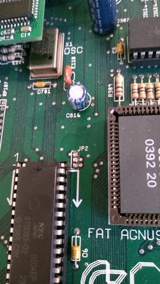
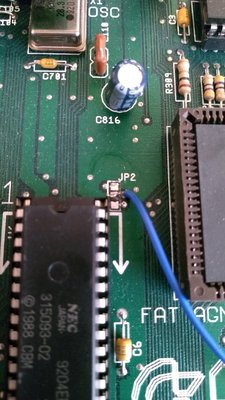
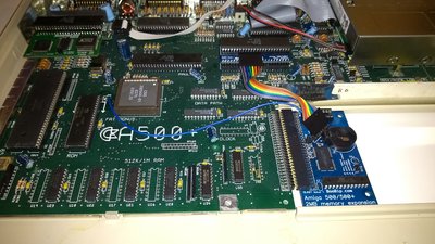
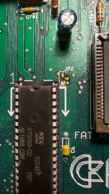
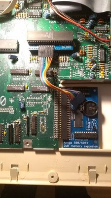
Today I recieved an 2mb chipmem upgrade for my Amiga500, and I have a small issue regarding installation. So I am hoping that someone here, have seen this product and know a bit about the installation procedure. That said... The upgrade that I have bought is this one: http://www.boobip.com/hardware/A500_2MB/installation and the idea is that I install the Gary adaptor, connect the adaptor to the memory board and finally solder jumper wire to JP2 on the Amiga board. Finally cut the trace between jumper-pads 2 and 3 on JP2.
The Amiga500 that I have, is one of those Rev 8a.1 boards, wich in reality is an Amiga500 Plus, refitted to be an standard 500. In reality, an 500 plus, with clock circuit and battery removed, memory reduced to 512kb and with KickStart 1.3 instead of 2.0 yet the chipset is the full ECS with 1mb Agnus and so on.
Now...
As far as I know. The classic chipram mod, requires the two upper pads to be bridged, and a solder blob between pad 1 and 2. And then some other mod's to another jumper and cutting a second trace somewere. (That is if there is no gary adaptor used, wich I have now).
Anyhow.
I have installed the memory module, and I have installed the Gary adaptor, and finally I need to solder the jumper wire on JP2 plus cut the trace between pad 2 and 3. As of now, the trace is not cut and there is a colder blob, bridging pad 1 and 2. Wich seems a little odd to me.
To boil it all down. The question is if I just remove the solder blob, cut the trace and solder the wire to pad number two? And why is pad 1 and 2 bridged and the trace between pad 2 and 3? Is that standard from the factory?
I have taken a picture of the mem upgrade in place in my 500, and a picture of JP2 just for reference to my question/issue.
Don't eat stuff off a 15 year old never cleaned cpu cooler.
Those cakes make you sick....
My blog: http://to9xct.blogspot.dk
My YouTube: https://www.youtube.com/user/brostenen
001100 010010 011110 100001 101101 110011