Reply 40 of 108, by stamasd
Rank
l33t
I'll measure mine when I get home, but I'd say probably 15-16 inches.
I/O, I/O,
It's off to disk I go,
With a bit and a byte
And a read and a write,
I/O, I/O
I'll measure mine when I get home, but I'd say probably 15-16 inches.
I/O, I/O,
It's off to disk I go,
With a bit and a byte
And a read and a write,
I/O, I/O
Ahh, monstrous -- like the Roland LAPC-I. Yeah the Tandy 1000s can't fit larger than 10" cards.
Yes it's as big as ISA cards can be.
I/O, I/O,
It's off to disk I go,
With a bit and a byte
And a read and a write,
I/O, I/O
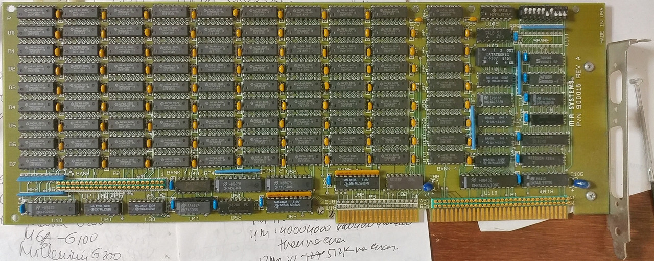
Log of today's activities with the "M A Systems" card.
Switch 5 on, all others off, same result as with all off.
Switch 6 on, all others off -> computer doesn't boot. 😀
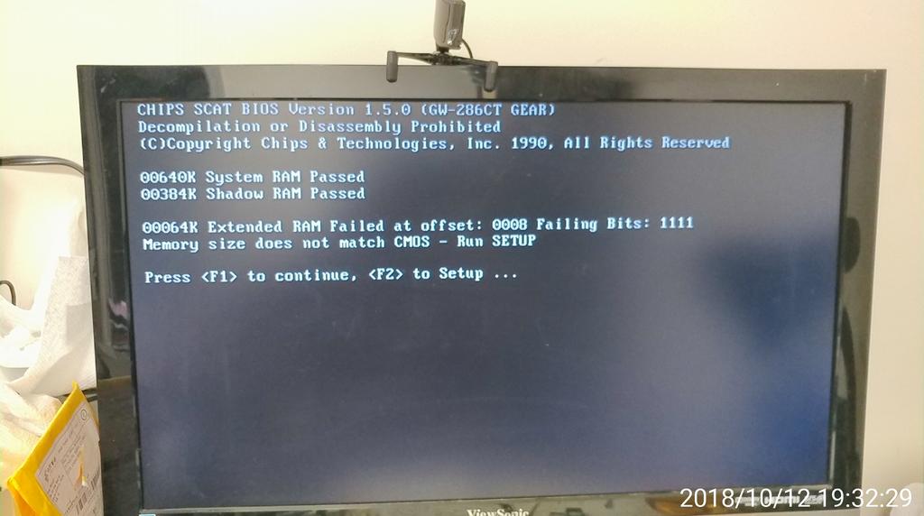
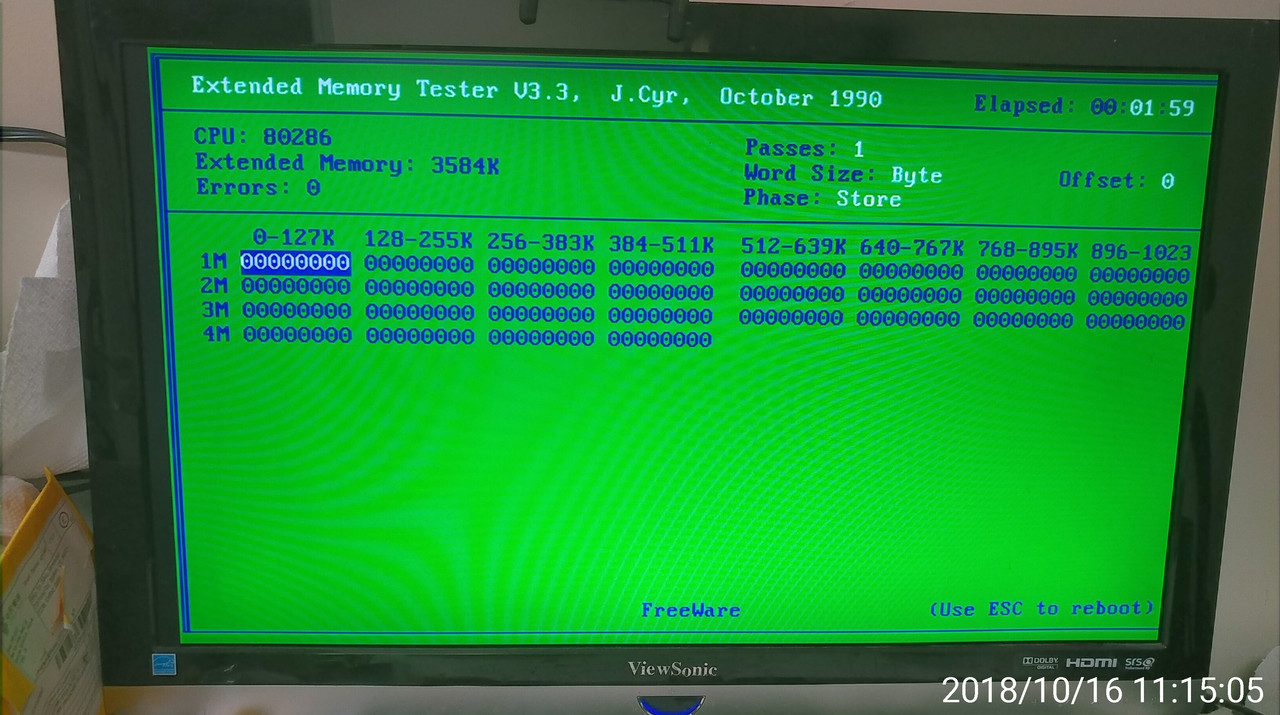
Switch 7 on, all others off -> 3072kB extended RAM recognized at boot.
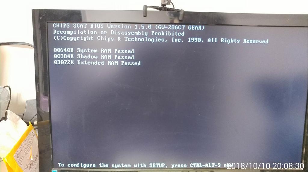
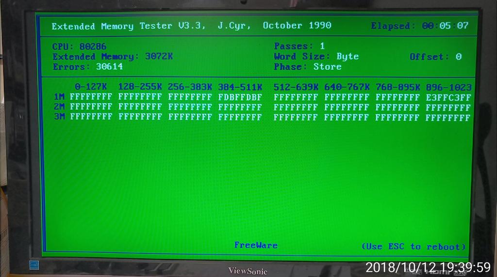
The test is a bit puzzling:
The tester program sees some memory in the first MB above 1M, but also a lot of errors. How did the BIOS recognize it all then?
I tested again the same configuration after a power cycle, and it gets even more puzzling.
Scratching my head here.
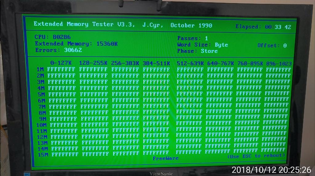
Switch 8 on, all others off:
Test:
Switch 9 on, all others off: same as with all switches off
Switch 10 on, all others off: parity error
So at least the role of switch 10 is clear. Off=enable parity, on=disable parity.
Gonna leave this here for now. Head hurts. Need sleep.
I/O, I/O,
It's off to disk I go,
With a bit and a byte
And a read and a write,
I/O, I/O
More tests.
All switches off except 5 and 6
All switches off except 6 and 7 - no boot
All switches off except 6, 7 and 8 - no boot
All switches off except 5, 6 and 7
Eventually it will make sense.
I/O, I/O,
It's off to disk I go,
With a bit and a byte
And a read and a write,
I/O, I/O
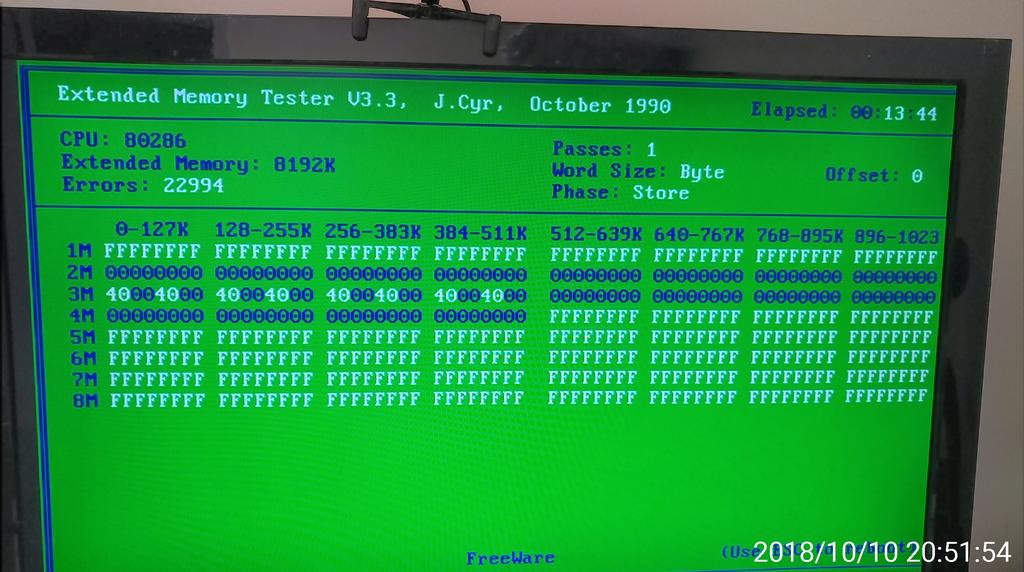
So to sum up the results so far: switches 1-10 xxxx-xxxx-xx
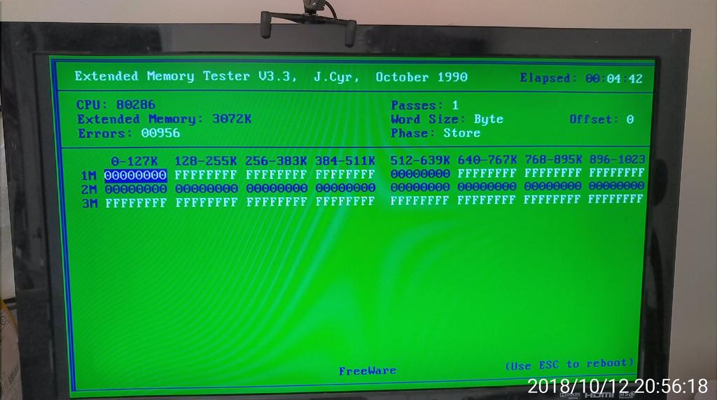
a. 0010-0111-11: 2.5M at 8M, 1 defective chip in 9M region
b. 1111-1111-11: no XMS
c. 0000-0000-00: 3.5M at 1M, same defective chip at 3M
d. 1000-0000-00: same as c
e. 0100-0000-00: same as c
f: 0010-0000-00: same as c
g: 0001-0000-00: same as c
h: 0000-1000-00: same as c
i: 0000-0100-00: no boot
j: 0000-0010-00: 3.5M at 2M, with 1 defect at 4-4.5M and another questionable region at 1M
k: 0000-0001-00: 3.5M at 2M with defect at 4-4.5M
l: 0000-0000-10: same as c
m. 0000-0000-01: parity error at boot
n. 0000-1100-00: 3.5M at 9M with 1 defect at 11M and questionable block in 7M area
o. 0000-0110-00: no boot
p. 0000-0111-00: no boot
q. 0000-1110-00: 3.5M at 9M with 1 defect at 11M and questionable blocks in the 7M, 8M regions
switch 10 toggles parity apparently (doesn't explain #a though)
switch 7 seems to swap in some memory in the megabyte before the 3.5M that show up constantly.
switch 6 seems to lead to some memory being paged where it shouldn't be (in the first megabyte perhaps, conflicting with the onboard RAM) except if switch 5 is also flipped and then the card's memory appears above 9M.
I have no idea what switches 1-4 do. Same for 9, and 8. Well 8 in one instance moved all RAM by 1MB up.
I/O, I/O,
It's off to disk I go,
With a bit and a byte
And a read and a write,
I/O, I/O
Your results are weird, especially the working bits "00000000" inside the "FF"s at the start in the latest screenshot.
I would propose you disassemble the daughter-board before continuing. There will be no way around as you have to fix that defective chip.
I think you weird results maybe related to that. I also observed this with one of my cards. After replacing the damaged chip with a working one the results were much clearer.
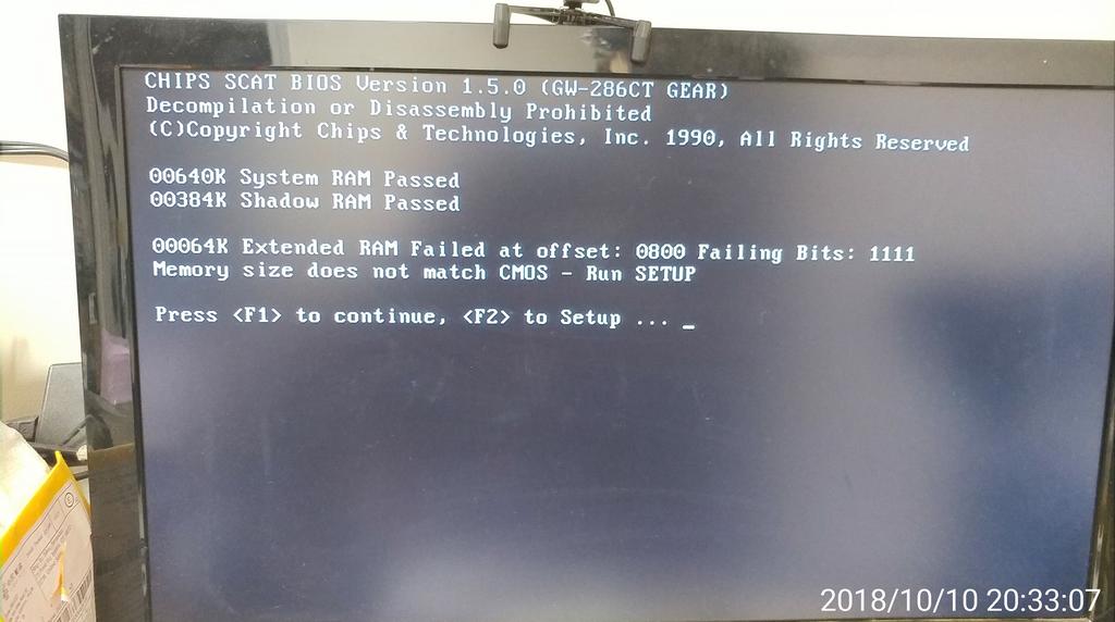
OK I have now removed the daughterboard. I just started testing, but I can see a significant change already. With all switched off and without daughterboard, the system only recognizes 1024k extended memory instead of 2048k. I wonder if the memory on the daughterboard and the one on the baseboard aren't interleaved.
I/O, I/O,
It's off to disk I go,
With a bit and a byte
And a read and a write,
I/O, I/O
After running some tests with the baseboard only, I can see some patterns... they don't make sense yet, but they're there. And they're similar to the tests ran with the daughterboard attached.
a. all off, 1024k found at boot, 1024k tested good after the base 1M
b. sw6 on all others off, doesn't boot
c. tests with only a switch on and all others off: (only one of sw1, sw2, sw3, sw4, sw5 was on) all show same as #a above
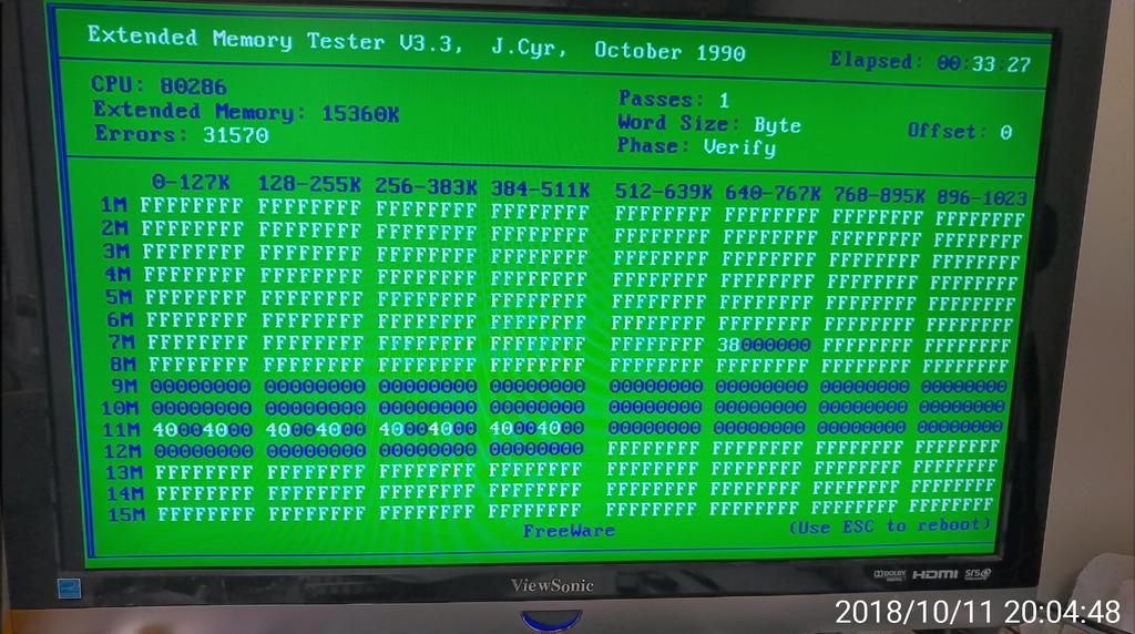
d. sw7 on, all others off: 2048k XMS counted by the motherboard at boot; testing shows this:
e. sw8 on, all others off: boot screen (seems like XMS is detected at boot but tests bad, not like other tests where XMS isn't detected at all)
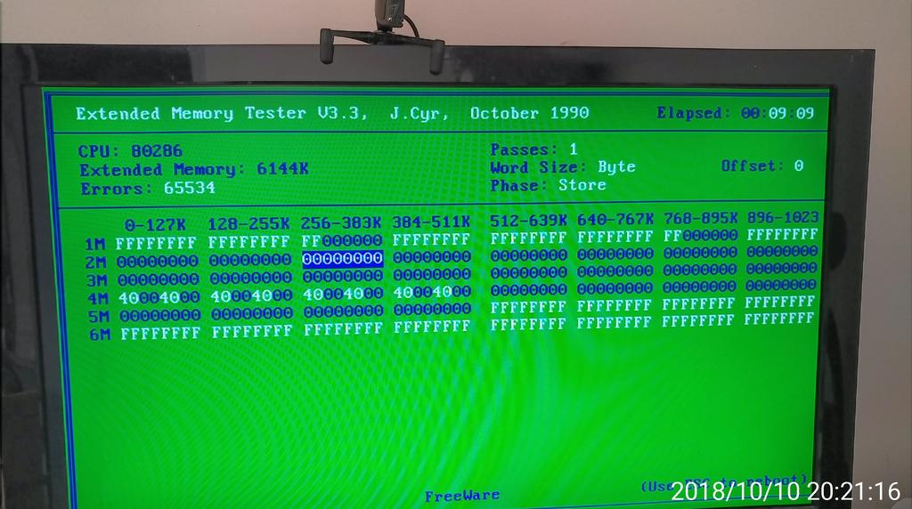
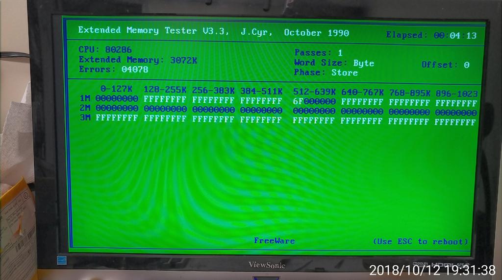
Quick test of this configuration covering only 3M XMS:
Notice some weirdness in some blocks on the 1M line.
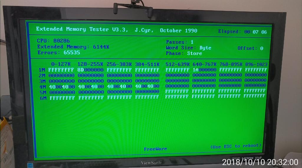
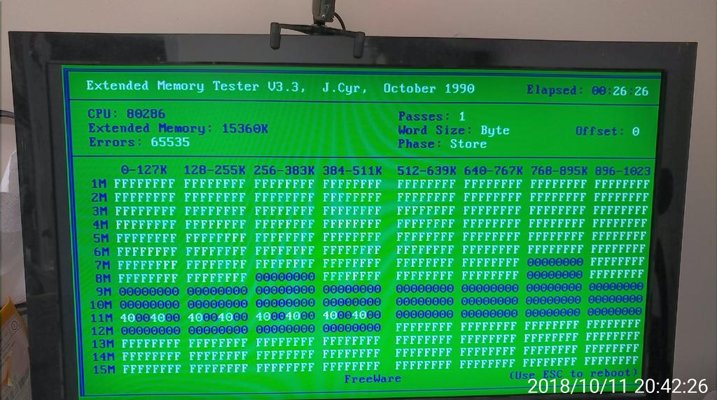
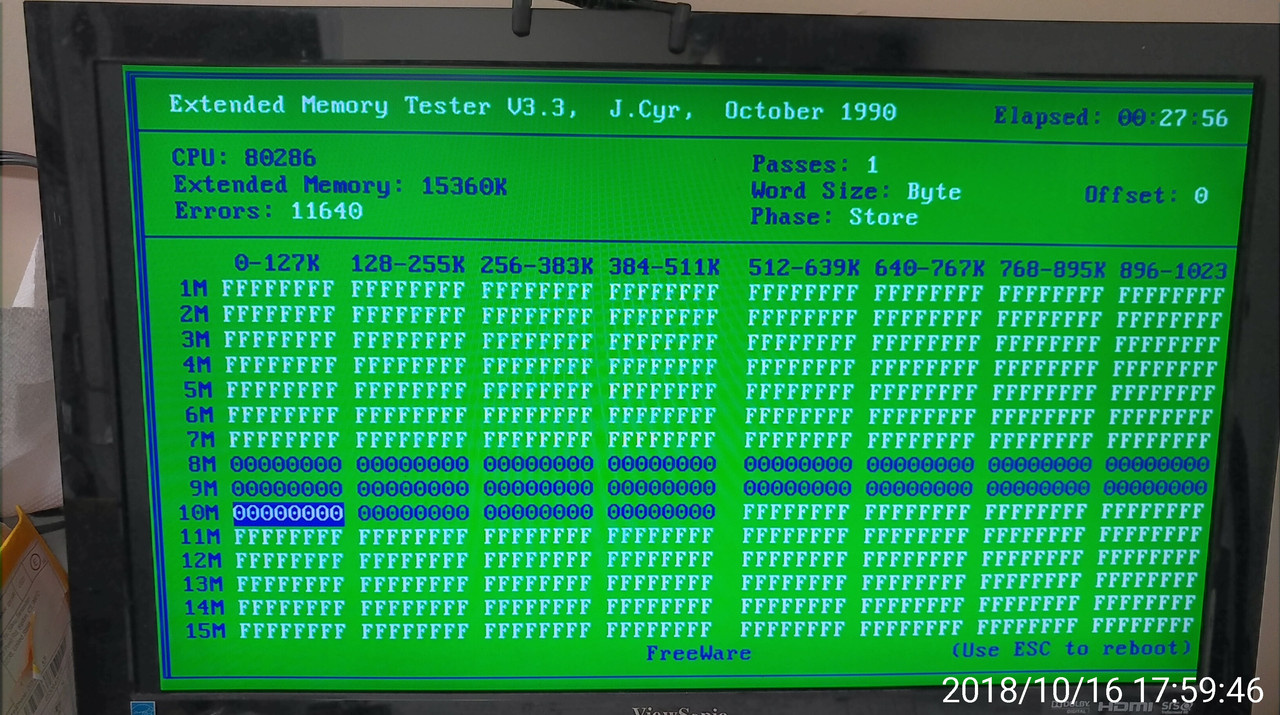
Tested again after power cycle, this time full 16M:
sw8 is weird. Moving on.
f. sw9 on, all others off: same as #a above
g. switches: 1,2,3,4 all on, all others off: same as #a above
h: switches 1 to 5 on, 6 to 10 off: same as #a above
i. switches 1-5 on, 6 off, 7 on, 8-10 off: again 2048k XMS counted by motherboard at boot, then this:
Compare to #d, see similarities: I saw a similar behavior for switch 7 in the tests with the daughterboard attached, see previous posts.
I still have no idea what switches 1-5 do; they seem to have no effect. 6 prevents boot unless 5 is on also (prev post), 7 brings online some blocks of memory but not others, 8 behaves strangely, 9 is like 1-5.
At least the line with the defective chip doesn't show up anymore so the chip that needs replacing is probably on the daughterboard.
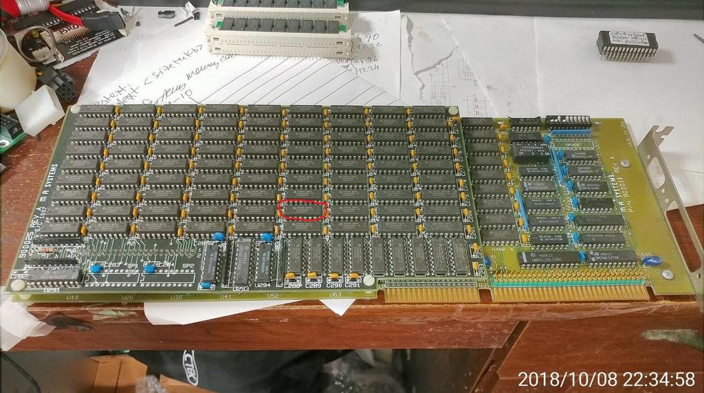
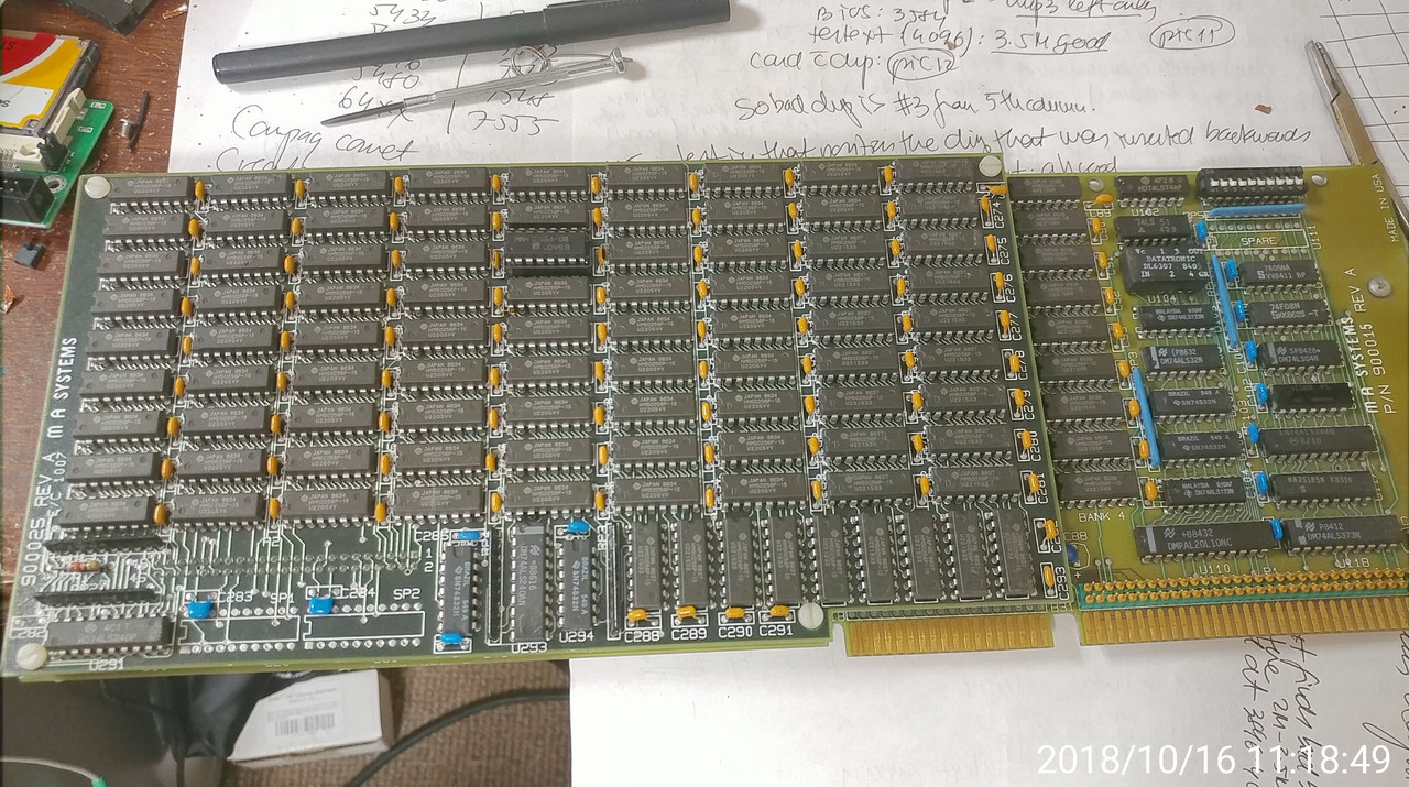
Oh yes and a picture of the card without the daughterboard:
Notice how the connector between the 2 boards is labeled "optimizer" 😕
I/O, I/O,
It's off to disk I go,
With a bit and a byte
And a read and a write,
I/O, I/O
At least you can see the layout, Bank 0-4 and bits D0-D7 plus parity.
I would propose you start with the initial configuration and try to locate this defective chip. Maybe you can piggyback a working one before desoldering to test.
For DIP testing, I would not use "all on" or "all off" as basis but a working configuration (the initial one...) and see what happens. Make small steps 😉
If I had an infinite amount of time just for this one project... But stuff has been piling up while I do all the testing, and I have one big thing coming up in a few days.
Considering that I already have made more memory show up than in the original configuration (ignoring the defective chip, 2.5M located in an unusable spot vs 3.5M right at the 1M boundary) I'm already close to calling it "good enough". If I repare that chip and get 3.5M XMS become usable I think I'll call it a day.
I/O, I/O,
It's off to disk I go,
With a bit and a byte
And a read and a write,
I/O, I/O
As far as testing by piggybacking chips, that may not be safe to do as these are CMOS chips not TTL. Without going into too much technical detail, here is why.
The output stage of a TTL chip has a high impedance path to Vcc, and a low impedance path to GND. By default the high impedance path to Vcc is "on" therefore the default state of the TTL output is a high-impedance logic "1". The output goes to a low-impedance logic "0" when the chip tells it to do so. Therefore tying together the outputs of 2 TTL chips, one of which is "0" and the other "1" whereas not recommended, will not create a short between Vcc and GND. This is for regular TTL outputs, not open-collector or TSL types.
For CMOS things are different. The output stage of a CMOS chip (regular output stage, not open-drain - but these memory chips don't have open drain outputs AKAIK) creates either a low-impedance path to Vcc for logic "1" or low-impedance path to GND for logic level "0". Tying together 2 regular CMOS outputs, one of which is "1" and the other "0" will create essentially a short between Vcc and GND which will draw high currents and probably destroy the output stages of both chips.
TTL output, notice the resistor to Vcc which limits current:

CMOS output, no limiting resistor (these outputs aren't supposed to have high currents flowing through them as normally either the upper or the lower transistor are OFF while the other is ON):

I/O, I/O,
It's off to disk I go,
With a bit and a byte
And a read and a write,
I/O, I/O
Anyway, I'm going to start chasing the defective chip. Won't have much time today or tomorrow - maybe Monday.
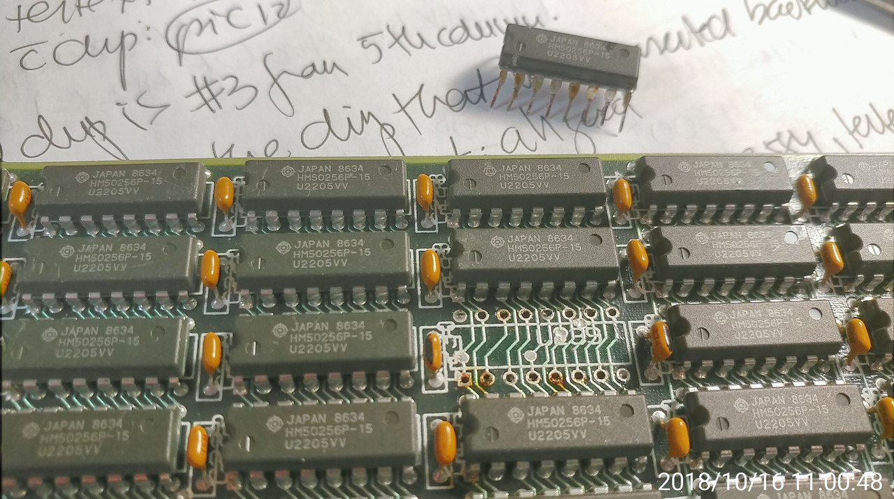
According to my calculations, the #1 suspect would be the chip providing the MSB-1 in the third bank on the daughterboard. This one maybe?
I/O, I/O,
It's off to disk I go,
With a bit and a byte
And a read and a write,
I/O, I/O
Yes, seems to be a rather reasonable start.
With all switches to "off", you only see 1MB. Thats the amount on the baseboard in this configuration.
With board, 3.5M XMS seen, of which 2M can be used due to the defective chip.
That means 2.5MB on the board, defective chip in the middle bank.
4000 hex = 0100000000000000 --> ROW D6
Yes, take this one. And test without this chip before soldering a new one 😉
Thank you for the confirmation.
BTW one thing that I wanted to mention which is probably not apparent from my poor phone pictures is how solid and beautifully constructed this board is. Including all contacts and connectors plated in thick gold. A recycler's dream, fortunately saved from that fate. It probably came from either a high end workstation or application-specific industrial machine.
I/O, I/O,
It's off to disk I go,
With a bit and a byte
And a read and a write,
I/O, I/O
OK against my own warning of danger, I did proceed to test with the piggyback method. I figured at most I'd be risking one loose RAM chip.
Unfortunately I didn't get any result with that. I tested the location in cause, followed by all locations on the same row, the row above it, and the second and third row from the top on the daughterboard (because I wanted to account for possible different organization of the memory on the daughterboard, where banks aren't marked) I also tested all locations on the 1/2 bank placed horizontally below the others. None of these made the error disappear. Happy to report though that the chip I used for testing survived and is still functional.
I thought maybe the output drive isn't enough to overcome that of the defective chip. To account for that, I tested the suspected location and a few others using 3 new chips piggybacked on top of the location tested. Still no result.
I/O, I/O,
It's off to disk I go,
With a bit and a byte
And a read and a write,
I/O, I/O
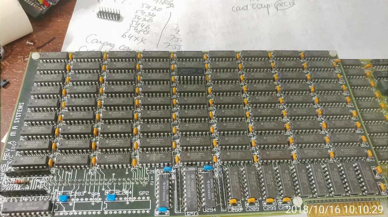
I've come back to report success. The board is repaired. 😀
I started this morning another series of tests, this time using a carpet-bombing technique. I took 9 good RAM chips and started piggybacking a whole column of chips on the daughterboard at a time, starting with the first on the left. I was intentionally sloppy in my piggybacking technique, hoping to introduce new errors during testing so I can figure out the layout of the memory banks. It worked.
I started seeing new errors in different regions of the memory, and the errors started moving around as I moved the piggyback chips to the right one column at a time. I won't post many images here though I took pictures of everything. Eventually I started seeing new errors in the same region of the memory with the defective chip, and that's when I knew I had the right column. That was the 5th column from the left.
I then started removing chips one by one from the bottom of the column, then from the top until I isolated the chip which would correct the original error when piggybacked (with good technique this time). It was the 3rd chip down from the top of the 5th column (dammit the 5th column strikes again like in the Spanish civil war).
When this was confirmed, I proceeded to unsolder that chip, solder a 16pin DIP socket and installed a good chip in it. The board tests good with 3.5M of XMS now.
The location that was defective with good chip piggybacked
Testing result in that location
Bad chip out
Socket with good chip in
Final test to confirm repair
Interesting observations based on the physical location of the chip relative to the memory error it was generating:
1. the order of the chips in each column is reversed on the daughterboard as opposed to the mainboard. I.e. the MSB is at the top, LSB at the bottom, parity bit still at the top.
2. The row of chips at the bottom of the daughterboard is probably part of the first bank as the bad chip was found in the 5th column instead of the 6th as I expected.
Anyway I have now a working board with 3.5M usable XMS. I don't know where the other 1.5M are hiding but I spent enough time on this project so I'm going to leave it here for now.
I/O, I/O,
It's off to disk I go,
With a bit and a byte
And a read and a write,
I/O, I/O
Congratulations, good work 😎 You can see this chip is rusty. Only this one?
Maybe you can try again the starting adress at 8.0MB to be sure the missing memory is not hidden at the beginning.
The chip is not rusty. That is flux. I like excessive amounts of flux when soldering/desoldering. Especially the cheap desoldering braids from China, which work fine if you give them enough flux because they're dry (as opposed to the good ones which already have flux on them). So I dip them liberally in rosin while using them.
All the brown on the chip and on the PCB is rosin flux.
Before desoldering the chip could not be physically distinguished from any of the surrounding ones. That's why you can see some markings I made with permanent marker to make sure I don't desolder the wrong chip. 😀
I/O, I/O,
It's off to disk I go,
With a bit and a byte
And a read and a write,
I/O, I/O
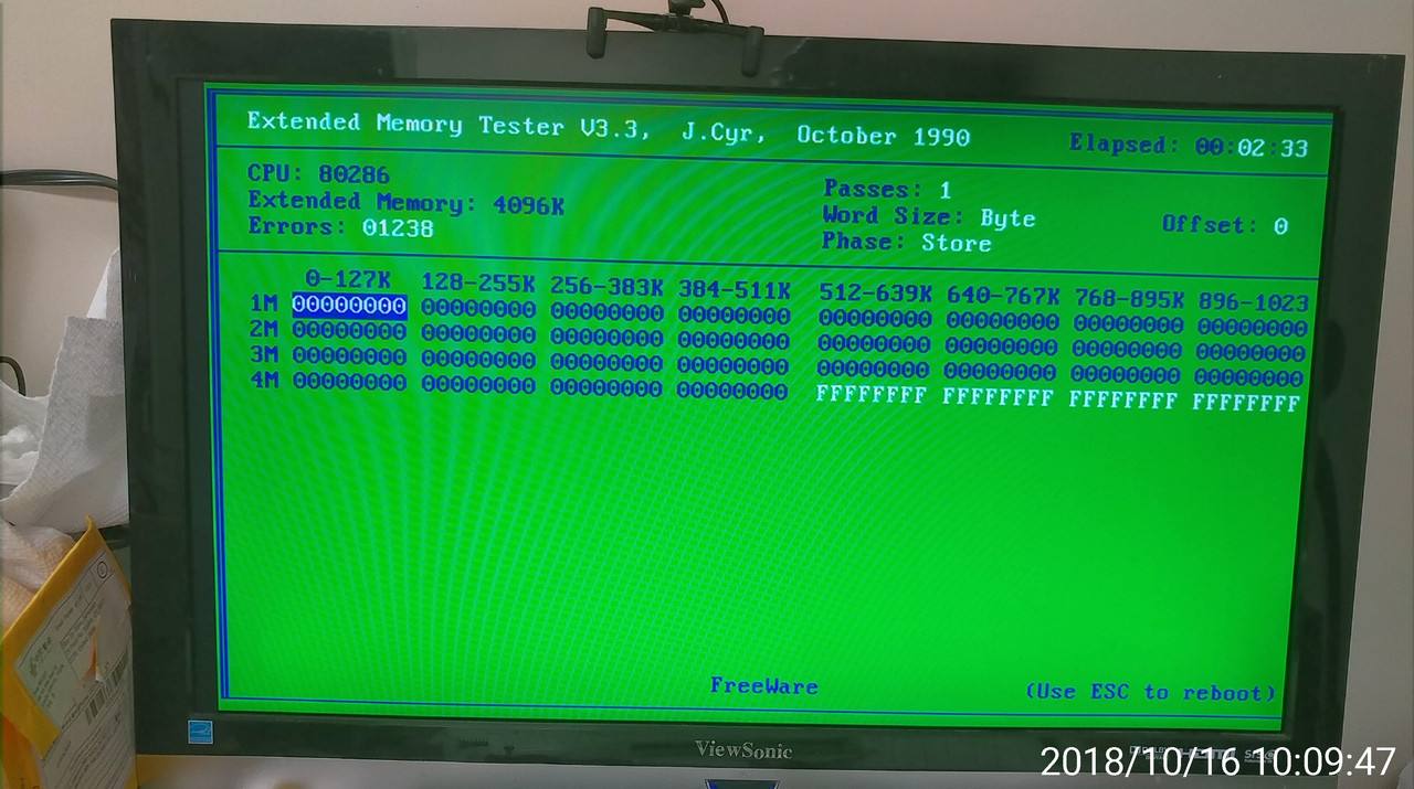
So I redid the full extended memory test after repairing the board with the switches in the original position. Nothing hidden.
I/O, I/O,
It's off to disk I go,
With a bit and a byte
And a read and a write,
I/O, I/O