VOGONS


Reply 20 of 33, by cosam

User metadata
Rank Newbie
Rank
Newbie
Paar wrote on 2020-03-14, 18:56:

You need UV light to erase that chip. Either you have specialized device that will erase within a an hour or so, or you could leave it outside for a week so a sun shines directly on it. Once it's erased you can program it however you want.

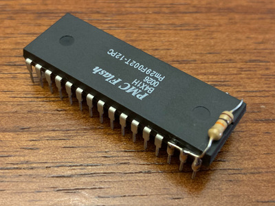
Yeah, I have neither the equipment nor the sunlight here 😁 Hence my preference to burn the right image in one go. A pin-compatible flash chip would have been ideal to experiment with but I've had no luck finding 64K x 8 in anything other than DIP-32.

Anyway - thanks for posting the image, can't imagine I'll need the memory hole option either. I'll check it out when I get a new EPROM.

PS. It turns out my VBS 1.06 is actually identical to yours. I originally dumped it from DEBUG.EXE so not sure where the corruption came from. Pulling the chip and dumping it using my programmer proved more reliable.

Reply 21 of 33, by cosam

User metadata
Rank Newbie
Rank
Newbie
cosam wrote on 2020-03-15, 16:28:

A pin-compatible flash chip would have been ideal to experiment with but I've had no luck finding 64K x 8 in anything other than DIP-32.

Turns out you can use a DIP-32 chip too, at least some of them. The PCB has holes for it but only a 28-pin socket. The "top" four holes are wired up like this, where 10K means +5V through a 10K pull-up.

+5V    =|  \__/  |=    +5V
10K =| |= +5V

This means that you can use (for example) a 256K x 8 chip, as long as the image is written to the top quarter. It would be neat to fit a 32-pin socket, or even just the four missing pins would be easier. I'd however rather not modify the board, so I replicated the circuit on the flash chip itself. The extra pins just hang over the edge of the socket. It would even be possible to write a second image and fit a switch on A16 to select. A17 is tired to VCC on the PCB in this configuration. Maybe there's a (hard) jumper to change that, I've not checked.

flash.jpg
Filename
flash.jpg
File size
215.61 KiB
Views
974 views
File license
Public domain

I took some time to compare the various images and tried to get as close as possible to the original VBS BIOS using the AH4 image. I also enabled a couple of hidden options, fixed some weird option layout issues and set a more informative description string. Pretty cool to see your own text when booting the machine 😁

This fixed the Y2K bug om my machine. Speedsys still complains that the rollover goes from 1999 to 1900, but the correct date is now saved, which is all I care about.

Attachments

  • Filename
    ah4-cosam.zip
    File size
    44.74 KiB
    Downloads
    54 downloads
    File license
    Fair use/fair dealing exception

Reply 23 of 33, by cosam

User metadata
Rank Newbie
Rank
Newbie
Paar wrote on 2020-03-16, 12:42:

I bought some DIP28 chips on eBay, it seemed there are plenty of them. Or could you use a site such as buyicnow.

Got part numbers? I figured I'd experiment with this setup and burn an EPROM when I'm sure it doesn't need more tweaking. Flash is a whole lot more convenient though...

Reply 25 of 33, by cosam

User metadata
Rank Newbie
Rank
Newbie
Paar wrote on 2020-03-16, 14:28:

Bought them from here

Ah, EEPROMs! Thanks, I was only searching for Flash. Can't go wrong at those prices so I have some W27C512 coming my way too. My Franken-chip will do fine until then.

Reply 26 of 33, by Hoping

User metadata
Rank Oldbie
Rank
Oldbie

Hello, sorry to reopen the thread to talk about something not directly related. It would be possible to see a close-up photograph of the area where the voltage regulator is, to know the values of the resistances around it, especially the blue ones.
Thank you very much

Reply 27 of 33, by cosam

User metadata
Rank Newbie
Rank
Newbie

Luckily for you I was just messing with this machine again and still have notifications on this topic! Hope that's clear enough for you.

Attachments

  • IMG_1825.jpeg
    Filename
    IMG_1825.jpeg
    File size
    1.1 MiB
    Views
    922 views
    File license
    Public domain

Reply 29 of 33, by Ayrton

User metadata
Rank Newbie
Rank
Newbie
Paar wrote on 2020-03-05, 15:02:
I have this nice and fully working motherboard Chicony CH-471B Rev 2.0: […]
Show full quote

I have this nice and fully working motherboard Chicony CH-471B Rev 2.0:

qra8l7ll.jpg

I want to use it with my 486 DX4 EW, which is a model with write-back L1 cache. Unfortunately, I cannot manage to make it work on this board with either jumper configuration (tried classic 486 DX4, then P24D), the CPU runs in WT mode every time. I have read this page and learned that it's possible to hardmod some boards to enable WB cache but the page mentions AMDs CPUs, not Intels. AFAIK AMD and Intel CPus have different pinouts so I'm not entirely sure it's possbile to use the page as proper instructions how to do it. I have checked the four necessary pins however and noticed that INV pin is not connected to any jumper. Possible cause of the issue?

Do you have an experience with these types od mods?

Hi, off topic but...
I am not lucky as you. I have the same motherboard, but ALL integrated controllers are gone! 🙁
As with external ISA cards all is working, could I ask you if you are using FPM RAM with "parity" or "not parity" modules?

My mobo is whimsical with RAM, do not know if it is related to integrated controller damage, and BANK2 out of order.
As I have to purchase RAM, it will be very appreciated if you could suggest me to buy "parity" or "not parity" module, cannot
find more detailed manuals than what I have now. Tests I made get me in confusion...

Thank you in advance!

Reply 30 of 33, by Paar

User metadata
Rank Member
Rank
Member

Too bad your's have integrated chips gone but that shouldn't be much of a problem, it's otherwise very nice and stable board. I'm using it even now and am very happy with it. I'm pretty sure I use non-parity modules, two modules of 8MB FPM RAM. I have used 4 of those modules without a problem but reverted to two as 32MB for 486 is overkill. I'm keeping those other two as spares.

There are lot of tantalum caps on this board. Could be helpful to check them all for shorts or replace them. They are time bombs after all.

Reply 31 of 33, by Robin4

User metadata
Rank l33t
Rank
l33t
Hoping wrote on 2020-08-17, 11:54:

Hello, sorry to reopen the thread to talk about something not directly related. It would be possible to see a close-up photograph of the area where the voltage regulator is, to know the values of the resistances around it, especially the blue ones.
Thank you very much

Some of those resistors are very hard to come by. Because they arent used anymore. How did you solved that?

~ At least it can do black and white~

Reply 32 of 33, by Ayrton

User metadata
Rank Newbie
Rank
Newbie
Paar wrote on 2020-12-19, 09:31:

Too bad your's have integrated chips gone but that shouldn't be much of a problem, it's otherwise very nice and stable board. I'm using it even now and am very happy with it. I'm pretty sure I use non-parity modules, two modules of 8MB FPM RAM. I have used 4 of those modules without a problem but reverted to two as 32MB for 486 is overkill. I'm keeping those other two as spares.

There are lot of tantalum caps on this board. Could be helpful to check them all for shorts or replace them. They are time bombs after all.

Thank you for your reply.
I risked to buy some FPM RAM yesterday and I bought only FPM non parity-modules 70ns (except 2 banks of parity ones at special discount price only to better understand this once and for all).
I hate to use partially faulted mobos, but once I understood what works and what does not, excluding failed stuff all the rest works good and regularly stable. BANK2 broken is a mystery...
Otherwise too many strange incompatibilty issues using BANK0 and BANK1, I hope I did not waste money yesterday...
When I have clean ideas of what types of RAM works I will write here to thank you for your attention...
PS: My mainboard came in my hands with battery fully charged, working, no signs of aging... and looking at it, it does not seem really to be produced 26 years ago... uhm... yours?

Cheers! 😀

Reply 33 of 33, by Paar

User metadata
Rank Member
Rank
Member

I think mine board is really vintage, it has all those old parts and looked old when I got it. Considering the non-working BANK2, check the underside for cracked solder, it can happen sometimes when one is not careful enough when installing memory modules. Generally, you should check for contiunity errors.

And definitely check the internet for supported memory configurations. It's possible the board won't work properly when installing memory only in BANK2. But I'm only guessing here, I would need to test it myself.