Reply 20 of 20, by kikipcs

- Rank
- Newbie
Update and some notes for me -
1. Who knew that I could reinforce the damaged pads using a bit of a copper foil tape? Gonna do that for a few more pins I think. For others, I’ve scavenged some pads from a donor P4 board, and epoxied them in place:
Epoxied resistor/cap row pads. We’ll see how that will end up. I'm only worried that the heat will melt the epoxy. IF the pads do not survive I'll make new ones, out of that copper foil tape. Gonna use short heatup, and a smaller temperature on my iron for these (~300*C)
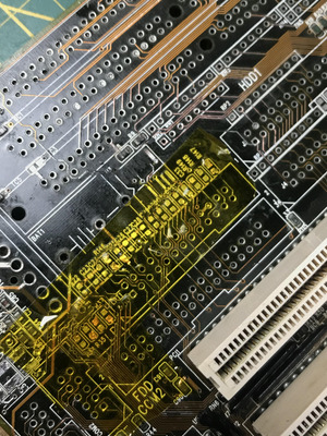
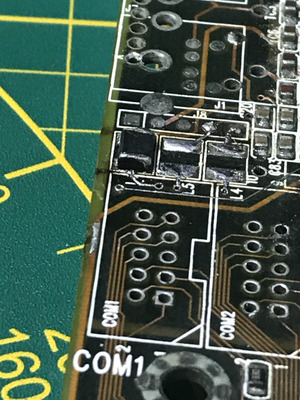
2. Went over the KBC and power circuitry, as well as the Super I/O chip area.
It's going well and I am putting kapton tape over finished areas to not distract me too much. I tend to look everywhere but the area I'm focusing on and I always spot a bit of solder here, a trace that could use a tin there... But a multimeter is my friend and were eyes may deceive you, a solid beep of reassuring continuity will not.
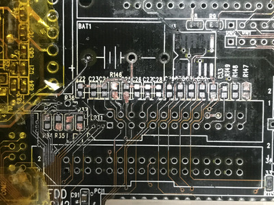
3. Big black SMD cap is too far gone. You can see it in the pic that there is almost nothing to solder to! And to make things worse, I don't know the values of it. From top side it goes to ground through a capacitor (it reads C20 I think), confirmed through a via on the underside, and by testing continuity from the top side to a screw point that is a ground. Yt’s also connected via C21 (capacitor right to C2, the one where it goes to the.. clock? Or reset? (If clock then it may not work. Dunno where is the clock – on the chipset?)
From the bottom side it goes and goes and ends up at pin 39 of the unused keyboard holes. Now, for some keyboard controllers it’s "T1", for others it’s "KBDI" (KBD data input). For 8042 it’s "test". Thing is, I have no “external” KBC so does it really matter? Or, should I bridge the solderpads of that cap/use a generic filtering capacitor to maintain the connection? Hmmm…
To me, now, IF it poses any problems, then the problems will be centered around keyboard input and PS/2 port. It does not connect to the PS/2 header though, that’s interesting. Only to the nonexistent onboard PS/2 port. Maybe it has to do with the fact that the board has a silkscreen for two PS/2 ports?
All other traces/connections on the KB circuit are OK from the top … and the bottom too. That area is for now done.
So:
- KBC done
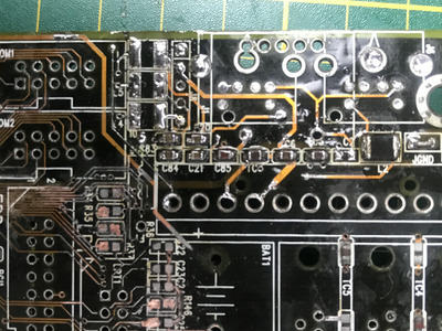
- Power circuit done
- Super I/O done
- COM ports done
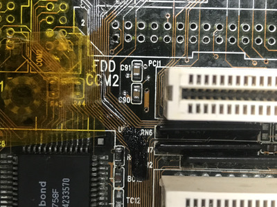
Next up is wiring up the traces for the SMD resistor/cap row. I'm using a 0,25mm kynar wire and it goes through vias with ease. Has anyone had any experience with using individual wire strands? You know, the tiny ones. I have a long, long cable from some old headphones and I've been sorta thinking about using it for those tight spaces.