First post, by 386SX
Hi,
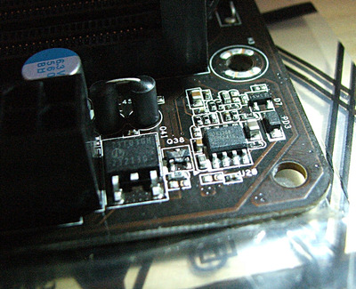
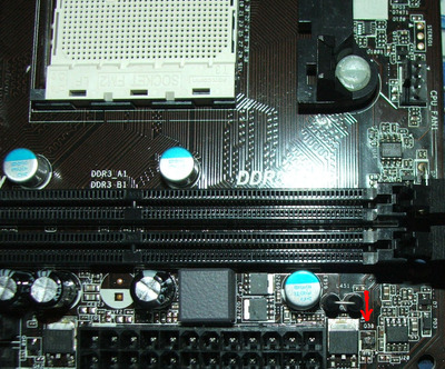
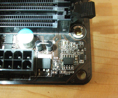
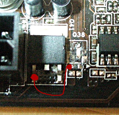
It's a long time I've this mainboard (FM2A55M-DGS rev 1.02) and never understood why it could not post; I tried cpu, rams, a new bios eeprom and at the end it became a personal quest to try understand the problem. At the end I think I found it: close to the ATX connector there's this component I never noticed it's sort of broken who knows what happened. I have already spent enough into this and I think I may replace it myself even if it's really not as big as it looks like so it's going to be difficult but the main problem is that I've no specifications or info about what was it in the first place. Have you any idea? If I think to all the time spent into the "usual" no-posting problems when most probably that may be THE problem...
Thanks!