jakethompson1 wrote on 2020-10-17, 19:33:
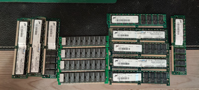
I have one of the same boards the OP is using and I remember running into an issue where it didn't beep when no RAM was in. Of course, I could have had something else messed up at the same time. Also, it seems sometimes those who didn't grow up with this stuff refer to all 72-pin SIMMs as EDO, so unless the OP has checked the chip datasheets I wouldn't bet on it.
I've wondered what it is about EDO that breaks these old pre-EDO boards though? Reading about it I thought it was supposed to be backward compatible. Is it an issue that only arises because a 486 board has both cache chips and RAM connected to the data lines at the same time?
No one mentioned EDO in this thread before me - I just mentioned it because this issue pops up regularly. And of course, EDOs are meant to be mostly compatible to FPM, but if they did behave exactly the same way, they would be FPM modules, not EDO modules. Specifically, this is the issue with EDO RAMs, which is exposed by a design choice in the 72-pin SIMM standard that turned out to be not that good with the advent of EDO SIMMs:
All modules (EDO and FPM) are 100% compatible to standard, non-page-mode RAM chips (they died like around 1988), because the "fast page mode" and EDO (also known as "hyper page mode") mode use access patterns, that are forbidden on non-page-mode RAMs. A non-page-mode read cycle works like this:
- The memory controller puts the row number on the address pins
- The memory controller asserts /RAS (row address strobe)
- The memory controller puts the column address on the address pins, replacing the column address
- The memory controller asserts /CAS (column address strobe)
- The memory chip drives the selected data from the chip to the I/O lines (single-bit data chips have dedicated input and output pins, but wider chips don't)
- The memory controller deasserts /CAS
- The memory chip stops driving the I/O lines, so they are free for other use
- The memory controller deasserts /RAS
This list does not included all the required delays between the steps, because describing all the timing requirements would make that list unreadable. There are two main take-aways from this list, though: First, when the memory controller deasserts /CAS, the next step by the memory controller will be deasserting /RAS. Second, deasserting /CAS causes the data to disappear from the data lines.
Now, introducing the "(fast) page mode" read cycle:
- The memory controller puts the row number on the address pins
- The memory controller asserts /RAS (row address strobe)
- The memory controller puts the column address on the address pins, replacing the column address
- The memory controller asserts /CAS (column address strobe)
- The memory chip drives the selected data from the chip to the I/O lines (single-bit data chips have dedicated input and output pins, but wider chips don't)
- The memory controller deasserts /CAS
- The memory chip stops driving the I/O lines, so they are free for other use
- The memory controller places a new column number on the address lines
- The memory controller asserts /CAS
- The memory chip drives the new selected data from the chip to the I/O lines
- The memory controller deasserts /CAS
- The memory chip stops driving the I/O lines, so they are free for other use
- The memory controller deasserts /RAS
The bold-faced steps are the additional steps to read another column from the same row (which is called "page" in this context for some unknown reason). Obviously, this is way faster than doing two complete cycles. This breaks with the first of the two observations on the non-paged cycles: In this case, the memory controller has the choice to not deassert /RAS, but re-assert /CAS after de-asserting /CAS. Chipsets starting with 286 chipsets kept /RAS asserted for some time after a memory cycle, so that if the processor requested another byte from the same row (aka page) in the next active memory cycle, it could be served in a "fast" way.
Later, system designers found out that this scheme has a limitation: Memory manufacturers specify a minimum time /CAS must be deasserted between cycles (they call it CAS recovery time). To get the maximum throughput, /CAS must thus be deasserted quite quickly after asserting /CAS, so that /CAS may be reasserted quickly. On the other hand, when deasserting /CAS, the memory chip must stop sending out the data to the bus, so /CAS must be kept asserted until the processor accepted the data. To increase performance, the access pattern was modified in a way that the reading of data by the processor may overlap with the memory chip preparing for a new column address. To achieve this, the point in time when the memory chip stops driving the data lines is no longer "when /CAS gets deasserted", but "when /RAS gets deasserted"! This means the processor can read the data while /CAS is high. As the time the data is output to the bus is extended, this modified pattern is called "extended data out" (EDO).
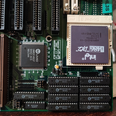
As explained in the paragraph before, starting with 286 chipsets, /RAS can be kept asserted even after a memory cycle ends (speculating for a "page hit" where the next cycle accesses the same page). If you replace FPM chips by EDO chips, the chips keep asserting data to the bus, so a bus conflict arises if a non-memory-cycle is performed while /RAS is still asserted. In case of cache-based systems (later 386 systems, nearly all 486 systems), cache-hits are cycles that can be perfomed while /RAS on the memory is still asserted. This is why EDO chips can break systems designed for FPM.
RAM chip designers were well aware of the problem that asserting data to a bidirectional bus depending on the chip state may cause issues (e.g. if a memory controller sends row and column addresses of a pending cycle while the data bits are still busy transferring data into a slow device), so they added an /OE (output enable) pin to the RAM chips, such that de-asserting /OE always makes the chip stop driving data to bus, no matter what the memory access timing protocol implies about outputting data. PC designers on the other hand found out that de-asserting /CAS happens naturally after a memory access, and this will cause the bus to get free, so they decided that the chipset does not need to drive the /OE signal; thus the /OE signal can be asserted permanently. This decision was driven by the pin count limit on standard IC cases at that time. Saving a pin for /OE for the RAM, and not needing to route a trace was a win for everyone. The consequence is that neither 30-pin SIMMs, not 72-pin SIMMs have an /OE signal, as it was not needed when these pinouts were defined.
Now that there are EDO modules, being able to remove /OE would be important to free up the bus while keeping a "page open" (keeping /RAS asserted), but it's impossible with SIMMs (EDO DIMMs added the missing signal). There are different ways to deal with that limitation, like introducing a three-state buffer between the RAM and the local bus that can be used to prevent RAM data being driven to the bus or by closing pages earlier such that conflicts on the bus are avoided (e.g. close a page not only on a cache-miss cycle that is a page miss at the same time, but also closing RAM pages when a cache hit occurs). EDO-compatible 486 mainboards have to employ one of these compensation methods to cope with the missing /OE pin at the SIMM socket. Some chipsets help with built-in support in the chipset, whereas other chipsets (like the SiS 496/497) require /OE to work to be EDO compatible.