First post, by rad

- Rank
- Newbie
Hi guys,
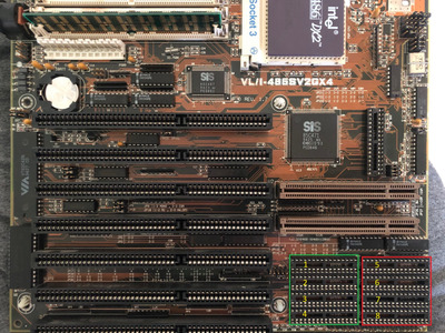
Recently I've acquired this motherboard (ASUS VL/I-486SV2GX4), Revision 1.7, without any additional voltage regulation (supports only 5V). The board was completely bare and stripped down, without any jumpers, bios, cache chip etc. Everything has been removed from it, so I've decided to give it a go and try to revive it.
The jumpers configuration of the board is different from those of 2.x revisions, more like revision 1.1 from here:
https://stason.org/TULARC/pc/motherboards/A/A … 6SV2G-VL-I.html
I've burned the latest BIOS (0402.001) from phils site on a new EEPROM chip, placed Intel 80486DX2/66 CPU (the only one that I've at 5V), VESA VGA card, some cache chips and some FPM ram and bam, the board started! Everything seems to be working fine.
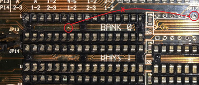
Actually not everything, because it turned out my L2 Cache is not detected during POST - it showed Cache: None. I've placed initially 4 128kx8 kbit SRAM chips (-15) along with one TAG 32kx8 (again -15) and set the jumpers to 512k cache. Nothing has been detected. Tried also with the same number and value of chips (128kx8) but this time -10ns (I've had them from 5 years ago when I was building my Cyrix 5x86 133 @2x66Mhz system) - and again - nothing has been detected. Also tried with some other spare chips (4x 32kx8 and one 8kx8) for 128k cache but again no luck.
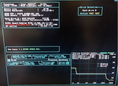
Tried downgrading the bios to from 04.02 to 03.03 and surprise - the cache has been detected! But it freezes the moment it tries to load MS-DOS. Either freeze or restart automatically. When I turn off the L2 cache in the BIOS it works great, I can run tests, programs, games, no problems whatsoever. But with L2 cache enabled it refuses to load the OS. Also what's odd is that with the 128k cache sometimes the BIOS detects it as 256k sometimes as 128k. What is also even more odd is that with 04.xx BIOS versions there is always an error for "keyboard not detected or faulty" at boot, but the keyboard is working fine, if I press F1 or DEL it continues, and on restart/reset it doesn't show that error. With older BIOS versions (03.xx) the message is missing at all and keyboard just works.
Unfortunately it is hard for me to take a full picture of the board as it is located in the tower AT case at the moment, but I've verified all jumpers positions and tried various other combinations. Probably it is still a problem with non-working cache chip, which later bios versions just automatically disable whole cache but older versions tend to try with it. I've ordered some 256kbit chips so that I could isolate chips problem (those chinese 128k -15 and -10 chips are unknown whether are working fine or not). I've tested all of them in a TL866-II programmer (with SRAM cache test) and they seem to work fine.
Any idea what could cause L2 cache issues? Faulty cache chips, bad socket/trace, chipset, CPU, Power supply?
Any help is appreciated,
Thanks!