VOGONS


IBM EGA Adapter Repair Advice Needed

Topic actions

First post, by FrankieKat

User metadata
Rank Newbie
Rank
Newbie

I have an original IBM EGA adapter that's experiencing some issues switching between resolutions - 320x200 ("Mode 1") and 640x350 ("Mode 2"). I am using an MCE2VGA adapter since I do not have an actual EGA monitor. First off, I have tried two DB9 cables, and have verified continuity between all 9 pins from the solder pins on each PCB so confident that there is no connection issue. I have also tried a different EGA card (a later "Paradise") which has no problems switching between resolutions with the MCE2VGA. I also have no problems using the MCE2VGA with a CGA and an MDA card, so that points to the IBM card as the source of the trouble.

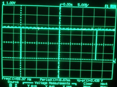
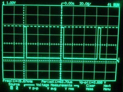
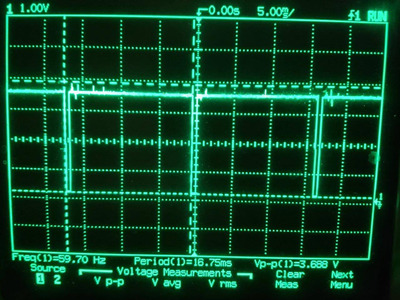
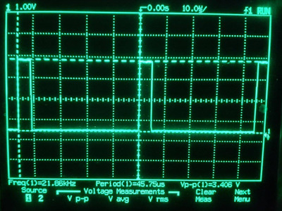
What happens is that the "monitor" stays in the 640x350 mode but continues to work and generate the correct graphics but is displayed out of sync and with incorrect color as you might expect. It's easy to see this on the MCE2VGA since there are LEDs that display the resolution that is currently being used - so the 640x350 LED (right most) will stay lit. It has worked correct from time to time, though I haven't been able to observe any correlation as to when/why. Otherwise it works perfectly and reliably in 640x350, both text and graphics.

There is one clue that I've seen and that is that there is a 74LS86 (quad XOR) gate chip (U8) on the schematic that gets very hot - measured at 153 degrees Fahrenheit. This gate appears to be used in the Horiz and Vertical SYNC and polarity circuit, and connects to the Horiz and Vertical pins on the DB9 output (via a 74LS244 buffer and a resistor). I checked for shorts between the gates on 86 and 244 and the resistor values and everything is okay there. It would seem odd that this temperature would be normal operating behavior, though I do not have another IBM EGA to compare. Near as I can tell, it's the only chip that's heating.

Any thoughts, ideas or tips would be appreciated. Obviously this EGA card is a rare beast, so would really like to see it repaired and working.

Thanks!

FK

Reply 2 of 20, by Deunan

User metadata
Rank Oldbie
Rank
Oldbie

I concur, it seems those two '86 gates are what generates final H/V sync signals in correct polarity. If the polarity is wrong (or the signal is distorted enough) you might not get a correct frequency detection on monitor side. Do you have a scope? You can just look at the signal before you do any soldering - that way you'll know if it's OK or not. An LS chip should not get hot unless it's shorted or driven with invalid logic levels.

Reply 3 of 20, by FrankieKat

User metadata
Rank Newbie
Rank
Newbie
Deunan wrote on 2021-05-12, 15:50:

I concur, it seems those two '86 gates are what generates final H/V sync signals in correct polarity. If the polarity is wrong (or the signal is distorted enough) you might not get a correct frequency detection on monitor side. Do you have a scope? You can just look at the signal before you do any soldering - that way you'll know if it's OK or not. An LS chip should not get hot unless it's shorted or driven with invalid logic levels.

I looked on a scope at the output pins 8 and 9 on the D-sub connector and compared them to the ones on MinusZeroDegrees , and the frequencies are dead on though voltages are a little low. All measurements taken with MCE2VGA connected. Not sure if the voltage measurements used on MZD were loaded with the monitor or not...

DB9 Output (looks right):

Mode 2 640x350 (working):
Pin f V
8 21.83 3.6
9 59.9 3.6

Mode 1 320x200 (not working):
Pin f V
8 15.7 3.6
9 59.9 3.7

74LS86 (U8):

Mode 2 640x350 (working):
Pin f V
1 59.97 3.7 VPOL
2 59.97 3.7 VSYNC
3 59.97 3.7
4 no signal HPOL
5 21.83 3.7 HSYNC
6 21.83 3.7

Mode 1 320x200 (not working):
Pin f V
1 no signal VPOL
2 59.97 3.7 VSYNC
3 59.97 3.7
4 no signal HPOL
5 15.7 3.7 HSYNC
6 15.7 3.7

The gate outputs (other than 1 and 4) however are very clean (if there's noise it's below what's visible on a 10V scale).

Suspect the lower as a symptom or the no signal on VPOL/HPOL from the LS273 flip-flop upstream?

Thanks!

FK

Last edited by FrankieKat on 2021-05-12, 18:51. Edited 1 time in total.

Reply 4 of 20, by Deunan

User metadata
Rank Oldbie
Rank
Oldbie
FrankieKat wrote on 2021-05-12, 17:31:

Suspect the lower voltages as a symptom or the no signal on VPOL/HPOL from the LS273 flip-flop upstream?

3.7V is well enough for TTL logic. Anything above 2.0V is logic H. The invalid range is between 0.8V (upper limit of L) and 2.0 (lower limit for H).

What does "no signal" mean - a steady level? What voltage exactly? Because frankly I would expect the polarity inputs to the '86 to be always H or L, depending on the mode, and not carry any signal (maybe some slight noise, that's it). The only thing switching fast should be sync inputs (and outputs, obviously). Basically the sync signals internally are always the same (just different frequency) and the XOR gates eiter passes it as-is or negates it, depending on the polarity input state. But then again I'm not familiar with internal workings of EGA.

Lets keep it simple for now - the outputs seem to have the right frequency and polarity on the scope, right? Nothing stands out as odd or malformed. And I would expect MCE2VGA to have TTL- compatible inputs as well - something to maybe investigate later if nothing else turns up. The difference, for the monitor and also MCE2VGA, other than frequency, is that V-sync is mostly L with H pulses (positive polarity) for 200 lines, and mostly H with L pulses (negative polarity) for 350 lines. Make sure that is the case.

With a scope it's easy to tell if the XOR gate is doing it's job - if the polarity input is L then the output should have exactly the same shape as input. With H level it will be inverted. So focus on the gate with pins 1,2,3 and check that.

Reply 5 of 20, by FrankieKat

User metadata
Rank Newbie
Rank
Newbie
Deunan wrote on 2021-05-12, 18:32:
3.7V is well enough for TTL logic. Anything above 2.0V is logic H. The invalid range is between 0.8V (upper limit of L) and 2.0 […]
Show full quote
FrankieKat wrote on 2021-05-12, 17:31:

Suspect the lower voltages as a symptom or the no signal on VPOL/HPOL from the LS273 flip-flop upstream?

3.7V is well enough for TTL logic. Anything above 2.0V is logic H. The invalid range is between 0.8V (upper limit of L) and 2.0 (lower limit for H).

What does "no signal" mean - a steady level? What voltage exactly? Because frankly I would expect the polarity inputs to the '86 to be always H or L, depending on the mode, and not carry any signal (maybe some slight noise, that's it). The only thing switching fast should be sync inputs (and outputs, obviously). Basically the sync signals internally are always the same (just different frequency) and the XOR gates eiter passes it as-is or negates it, depending on the polarity input state. But then again I'm not familiar with internal workings of EGA.

Lets keep it simple for now - the outputs seem to have the right frequency and polarity on the scope, right? Nothing stands out as odd or malformed. And I would expect MCE2VGA to have TTL- compatible inputs as well - something to maybe investigate later if nothing else turns up. The difference, for the monitor and also MCE2VGA, other than frequency, is that V-sync is mostly L with H pulses (positive polarity) for 200 lines, and mostly H with L pulses (negative polarity) for 350 lines. Make sure that is the case.

With a scope it's easy to tell if the XOR gate is doing it's job - if the polarity input is L then the output should have exactly the same shape as input. With H level it will be inverted. So focus on the gate with pins 1,2,3 and check that.

Sorry, "no signal" meant steady (low I assume but will re-check). There was a slight amount of noise yes. I'll re-measure what the PP on it was to be sure it was only slightly noisy. That was my thought as well that the polarity inputs to the gate should be either high or low, so perhaps I made an error there - I will re-check. That said, the polarities of the output signal do look right, so maybe that's not it...

With that in mind, I will re-measure all of the XOR pins on the gate and update.

Update: I measured DB9 output on my other EGA card (that works fine in 320x200 mode) and voltages were also right around 3.6V as well. Scope traces were effectively identical to the IBM one... hmph.

Meanwhile here are the scope measurements on the IBM from the DD DB9 video out. The frequencies and pulse lengths are right on spec, but voltages slightly low.

Attachments

Reply 6 of 20, by snufkin

User metadata
Rank Oldbie
Rank
Oldbie
FrankieKat wrote on 2021-05-12, 19:15:

Meanwhile here are the scope measurements on the IBM from the DD DB9 video out. The frequencies and pulse lengths are right on spec, but voltages slightly low.

Shouldn't Mode 1 Vertical be +ve going? It looks -ve in the scope trace, and the minuszerodegrees site gives only Mode 2 Vertical as -ve going.

In case it's useful, I had a go a looking back through the schematic for what controls VPOL and HPOL. My probably unclear notes are:
Working backward from U8

Sheet 9 - U8-1&4 (LS86) VPOL & HPOL <- U37 19&16 (LS273) <- BD7&6 (sheet 1)
<- clocked by MODE_IOW (sheet 4)

Sheet 4 - U25-1 (LS138) MODE_IOW, gated by pin 5 IOW (sheet 1)
also by pin 4, controlled by U34-14 (Q0)
controlled by A7..0

Sheet 1 - Slot1 B13 - IOW
BD7&6 -> U38-12&13 (pull up on BD)
-> U39-11&12 (LS245)
D7&6 -> U39-9&8 -> Slot1 A2&3

U39 direction set by pin 1 DIR (sheet 4 - logic net)

Reply 7 of 20, by mkarcher

User metadata
Rank l33t
Rank
l33t

Your scope traces clearly show that the output of the XOR gate, as observed on the DE-9 connector, is incorrect. Both in mode 1 and in mode 2, on your card VSync is active low and HSync is active high. This is wrong. In mode 1, VSync needs to be active high instead. -0° has a scope trace of the Mode 1 VSync signal as it has to be. It's exactly the job of that XOR gate to adjust the polarity of the sync pulses. I assume that "no signal" on Pin 1 in mode 1 means that Pin 1 is low (very close to 0V), whereas 3.7V in mode 2 means that the pin is high, although there shouldn't be a 60Hz signal on Pin 1, just on pins 2 and 3. If this is indeed the case, the XOR gate is clearly broken. Changing pin 1 from low (in mode 1) to high (in mode 2) should invert the polarity at pin 3, which it doesn't. Get a new 74LS86. A 74HCT86 will probably work well as substitute if that one is easier to get for you.

Reply 8 of 20, by FrankieKat

User metadata
Rank Newbie
Rank
Newbie
mkarcher wrote on 2021-05-12, 20:33:

Your scope traces clearly show that the output of the XOR gate, as observed on the DE-9 connector, is incorrect. Both in mode 1 and in mode 2, on your card VSync is active low and HSync is active high. This is wrong. In mode 1, VSync needs to be active high instead. -0° has a scope trace of the Mode 1 VSync signal as it has to be. It's exactly the job of that XOR gate to adjust the polarity of the sync pulses. I assume that "no signal" on Pin 1 in mode 1 means that Pin 1 is low (very close to 0V), whereas 3.7V in mode 2 means that the pin is high, although there shouldn't be a 60Hz signal on Pin 1, just on pins 2 and 3. If this is indeed the case, the XOR gate is clearly broken. Changing pin 1 from low (in mode 1) to high (in mode 2) should invert the polarity at pin 3, which it doesn't. Get a new 74LS86. A 74HCT86 will probably work well as substitute if that one is easier to get for you.

Yes, you are correct - somehow I missed that! Going back to my original post and @Deunan's comment about the xPOL signal should be either H or L but not pulsed, I re-checked the outputs at the gate. Indeed, when it is supposed to be inverted pin 1 does show an identical pulse to the pin 2, except at about 800mV, which would seem to again point to a bad/leaky XOR gate.

Okay, so sounds like I know what I need to do -- get that 74LS86 out of there! I may try to snip out those three pins and jumper over to one of the other unused gates to prove it while waiting for the new one to arrive.

Thanks for all the great tips and info!

FK

Reply 9 of 20, by maxtherabbit

User metadata
Rank l33t
Rank
l33t

The original EGA monitor (5154) strictly used sync polarity for mode detection. I'm not *surprised* that this would be replicated in a modern scaler, but it does seem a questionable design choice

Reply 10 of 20, by FrankieKat

User metadata
Rank Newbie
Rank
Newbie
snufkin wrote on 2021-05-12, 20:29:

In case it's useful, I had a go a looking back through the schematic for what controls VPOL and HPOL.

So I'm wondering what is the use case for HPOL being anything other than positive, since (as far as I know) all compatible monitors at the time worked that way? "Future proofing", just like their extremely successful feature connector and dual RCA jacks? 😀

I bodged over the vertical XOR gate to the unused one on the other side and the card switched right into Mode 1 just like it was supposed to! The only thing though is that the IC is still getting hot, so it's definitely a dud, but certainly helps confirm it is indeed the issue. I've ordered up a replacement for it and hopefully that should just do the trick!

Thanks again for all of the great help and really interesting info!

FK

Reply 11 of 20, by Deunan

User metadata
Rank Oldbie
Rank
Oldbie

It would be silly to create HW with just the things you thought of during early design phase, only to later find out there's issues you can't resolve without another HW revision or nice features that can't be implemented because you didn't add one more simple signal. EGA CRTC is pretty programmable, it's only logical to have HSync polarity if you already have VSync one.

As for mode detection, the reason polarity was used is because it's easy and saves one extra wire in the cable. With modern FPGA samplers one could try to detect the frequency but that's not as easy, and can fail on weird non-PC outputs (like say arcade boards, which during that time many had non-standard frequencies - close, but not exactly in spec). Granted, MCE2VGA is mostly meant for PC cards, but that doesn't mean we should exclude other machines. And even if your particular video output is not the correct polarity, adding an inverter gate to sync line is simple, tweaking the HDL code for different frequency ranges not so much.

Reply 12 of 20, by snufkin

User metadata
Rank Oldbie
Rank
Oldbie
FrankieKat wrote on 2021-05-13, 01:34:

So I'm wondering what is the use case for HPOL being anything other than positive, since (as far as I know) all compatible monitors at the time worked that way? "Future proofing", just like their extremely successful feature connector and dual RCA jacks? 😀

Using the second XOR for HSYNC could just be a convenient/free way of buffering it? Both HSYNC and VSYNC get buffered again by U76 before going to the 9-pin connector, but they're also directly connected to the feature connector (sheet 10), and the '86 would be cheaper to replace than the CRT CTRL chip (U32, sheet 3) that generates the sync pulses . Doesn't explain why they routed HPOL as a control for it though. Future proofing seems like a fair guess, or (I don't know the timings here) reusing a previous design.

I bodged over the vertical XOR gate to the unused one on the other side and the card switched right into Mode 1 just like it was supposed to! The only thing though is that the IC is still getting hot, so it's definitely a dud, but certainly helps confirm it is indeed the issue. I've ordered up a replacement for it and hopefully that should just do the trick!

Nice. Out of interest, are the inputs on that chip tied either high or low? I was taught that leaving inputs disconnected could lead to them floating around the switching voltage, leading to large currents flowing and overheating. If that's a problem in the real world then IBM must have connected them up. So I'm wondering if maybe there was a bad solder joint on an unused input causing a problem.

Reply 13 of 20, by Deunan

User metadata
Rank Oldbie
Rank
Oldbie
snufkin wrote on 2021-05-13, 10:26:

I was taught that leaving inputs disconnected could lead to them floating around the switching voltage, leading to large currents flowing and overheating.

That's true, and a good practice in general, but it applies mostly to FET technology (so anything MOS). TTL chips are based on bipolar transistors and the way inputs are designed there's always a pull-up resistor. Therefore it was common to leave TTL inputs not connected, these would not float but default to H level. It can be a minor issue if the TTL chip is replaced with a more modern HCT, but then again it's probably unused gate and HCT is pretty low power anyway, it would contribute to some noise but not really heat the chip.

Reply 14 of 20, by snufkin

User metadata
Rank Oldbie
Rank
Oldbie
Deunan wrote on 2021-05-13, 12:36:
snufkin wrote on 2021-05-13, 10:26:

I was taught that leaving inputs disconnected could lead to them floating around the switching voltage, leading to large currents flowing and overheating.

That's true, and a good practice in general, but it applies mostly to FET technology (so anything MOS). TTL chips are based on bipolar transistors and the way inputs are designed there's always a pull-up resistor. Therefore it was common to leave TTL inputs not connected, these would not float but default to H level. It can be a minor issue if the TTL chip is replaced with a more modern HCT, but then again it's probably unused gate and HCT is pretty low power anyway, it would contribute to some noise but not really heat the chip.

Ah, thanks, I must have been told that at some point but had forgotten. Just had a quick reread, so is the pull-up via current flowing through the Base-Emitter diode of the input transistor, whereas for FETs there's no current (other than gate capacitance) through the gate?

Reply 15 of 20, by the3dfxdude

User metadata
Rank Oldbie
Rank
Oldbie
FrankieKat wrote on 2021-05-13, 01:34:

So I'm wondering what is the use case for HPOL being anything other than positive, since (as far as I know) all compatible monitors at the time worked that way? "Future proofing", just like their extremely successful feature connector and dual RCA jacks? 😀

Actually... even though a feature is included in a product, it doesn't mean it was necessarily intended to be marketed to general home consumers. There almost certainly was a customer who requested the ability to perform video processing with their custom board attachment, to which IBM provided the feature connector. The EGA was offered as a high end expansion card when it was released, so the cost really wasn't an issue to include components to support it. And it doesn't matter that it didn't really have much use for the general consumer at the time. It is a myth too that IBM never had a use for it. They did release a product that uses it -- again out of the price range that any normal person would have considered it.

Now about those late EGA clone makers that included the feature connector, but breaking its function in the process, now that is kind of amusing to me.

Reply 16 of 20, by FrankieKat

User metadata
Rank Newbie
Rank
Newbie
the3dfxdude wrote on 2021-05-13, 15:09:
FrankieKat wrote on 2021-05-13, 01:34:

So I'm wondering what is the use case for HPOL being anything other than positive, since (as far as I know) all compatible monitors at the time worked that way? "Future proofing", just like their extremely successful feature connector and dual RCA jacks? 😀

Actually... even though a feature is included in a product, it doesn't mean it was necessarily intended to be marketed to general home consumers. There almost certainly was a customer who requested the ability to perform video processing with their custom board attachment, to which IBM provided the feature connector. The EGA was offered as a high end expansion card when it was released, so the cost really wasn't an issue to include components to support it. And it doesn't matter that it didn't really have much use for the general consumer at the time. It is a myth too that IBM never had a use for it. They did release a product that uses it -- again out of the price range that any normal person would have considered it.

Now about those late EGA clone makers that included the feature connector, but breaking its function in the process, now that is kind of amusing to me.

Interesting! I've done a little bit of searching but never came across any concrete examples of a production product that used the feature connector. What was it and what did it do?

And yeah, my later Logitech/Paradise EGA card has a "feature adapter" but a completely different connector and no RCA jacks so of course incompatible with an IBM one.

Reply 17 of 20, by FrankieKat

User metadata
Rank Newbie
Rank
Newbie
snufkin wrote on 2021-05-13, 10:26:

Nice. Out of interest, are the inputs on that chip tied either high or low? I was taught that leaving inputs disconnected could lead to them floating around the switching voltage, leading to large currents flowing and overheating. If that's a problem in the real world then IBM must have connected them up. So I'm wondering if maybe there was a bad solder joint on an unused input causing a problem.

Yes, the unused two gates on the EGA for that IC are completely disconnected on the PCB so I guess IBM was good with it. I also checked for shorts between all of the unused pins, and between +5 and GND and all were open, so no shorts or connections, and just left floating.

Last edited by FrankieKat on 2021-05-13, 17:52. Edited 1 time in total.

Reply 18 of 20, by the3dfxdude

User metadata
Rank Oldbie
Rank
Oldbie
FrankieKat wrote on 2021-05-13, 15:29:

Interesting! I've done a little bit of searching but never came across any concrete examples of a production product that used the feature connector. What was it and what did it do?

The IBM Infowindow touchscreen display (the original one, not the terminal computer). The feature connector was used for composite video sync (not for composite video itself, just uses dot clock input on the RCA jack) and detecting the presence of the proper display. So it requires essentially the original IBM EGA card, or the early direct clones. All the later cards are pretty suspect, although I think I heard the ATI EGA might have a fallback mode where it could function correctly.

FrankieKat wrote on 2021-05-13, 15:29:

And yeah, my later Logitech/Paradise EGA card has a "feature adapter" but a completely different connector and no RCA jacks so of course incompatible with an IBM one.

Yes, that defeats the original purpose. However, it could possibly be rigged up to drive an internal TTL or composite screen, but no one really did that at that point, and those machines already had their own plugs and compatible boards when they were sold. So this is why it was never used except for a few tinkerers. Really no home use, and for what it was used for probably never was available to the public.

Reply 19 of 20, by Deunan

User metadata
Rank Oldbie
Rank
Oldbie
snufkin wrote on 2021-05-13, 14:47:

Ah, thanks, I must have been told that at some point but had forgotten. Just had a quick reread, so is the pull-up via current flowing through the Base-Emitter diode of the input transistor, whereas for FETs there's no current (other than gate capacitance) through the gate?

In short, yes. A longer answer is also yes - except that it's not always a multi-emitter transistor but possibly just shottky diodes (LS series). Electrically it's almost the same thing, +/- a 0.1V or so, but it does affect the switching speed (and the value of the resistor is also different). Anything MOSFET based will act as a small capacitor due to parasitic properties of the gate, and that can randomly charge or even pick up signals from nearby circuits via RF or power delivery. There usually are protection diodes but these will have such a low leakage that the charge will not dissipate by itself. If it gets anywhere close to Vcc/2, it will cause all the transistors in the path to conduct, which basically creates a power to ground short-circuit at the gate output. It won't kill it due to limited amout of current but it will heat up, especially the LSI devices.

There is however a case where you want to keep the mean DC level at Vcc/2 on an inverting gate - RC or quartz oscillator. But these do not dwell at this voltage obviously, it's only a way to introduce a strong feedback. And again, if the oscillations were to stop the gates would start drawing more current but if the chip is a simple CMOS, in older tech like 4000 series, you probably won't notice any heating up. You might see the higher current draw if you could isolate the power to that chip alone though.

It can be a pretty complicated subject but the rule to have all unused inputs tied to something is a good one and should be followed even with TTLs. It's just with TTLs it wasn't really needed and you could wire the gates easier (no need to cut any traces) if necessary - so often these were left unconnected.