Reply 20 of 27, by FrankieKat
Rank
Newbie
mkarcher wrote on 2021-07-27, 16:48:In such cases, I usually scratch the solder mask from the copper traces on both sides of the break, and solder a thin strand of copper wire over the break, and fix/isolate the bodge with nail polish.
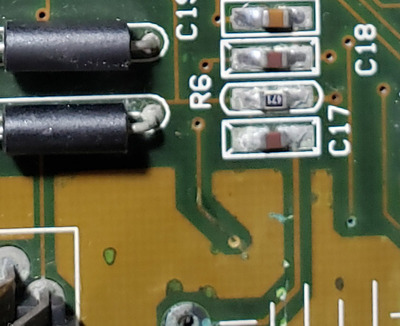
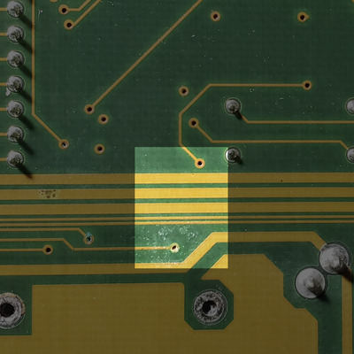
The via on the break itself is also damaged - if I probe it from both of it's sides, I get open so the top side of that is no use. Shortest fix I think will be on the bottom side of that trace (pictured below). I've got some 26 AWG bodge wire, do you think I could remove the solder mask on those vias (lacquer thinner?) tin the wire, solder it into the via cup and adhere it down? Those traces are tiny in real life!
FK