First post, by leency
Rank
Newbie
Hello everyone,
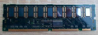
Could anyone please help to identify this DIMM RAM? Is it a specific one or a common unit with just a specific form of chips?
Regards
Hello everyone,
Could anyone please help to identify this DIMM RAM? Is it a specific one or a common unit with just a specific form of chips?
Regards
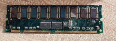
The keying indicates it's unbuffered 3.3V, which could be EDO or SDRAM, the 9 chips indicate parity/ECC and those extra chips below the DRAM show it's registered.
There's an SPD EPROM, which is mandatory for SDRAM and optional for EDO. My guess given the colour and design is it would be SDRAM, but can't be 100% certain. In any event there's nothing written on the chips to go by. If you have it, put it in a motherboard supporting registered SDRAM and see if it gets detected and if so what the SPD says.
To me it looks like registered ECC SDRAM.
See also
Converted registered SDRAM
RAM for IBM PC 365 Dual Pentium Pro
BTW, I wonder whether registered unbuffered RAMs can exist... isn't both mutually exclusive?
If that unit doesn’t work in your motherboard (which it probably wont in most being registered) check out the link in the last reply. Post there and I think they can help you unregister it
Btw, lemme know if you figure out what those are called that looks really cool!
Probably won't work properly, if at all atm due to the busted chip legs on 1,3 & 4 from the left
It looks as if someone removed the ram chip top covers or something?
It looks like it's just bare silicon.
PC Hoarder Patrol wrote on 2021-11-08, 10:34:Probably won't work properly, if at all atm due to the busted chip legs on 1,3 & 4 from the left
On top of that, one if the resistors (second from the left 1st line) seems like it's not in line with the other resistors.
Could this be some regular SDRAM which has been tampered with and now looks like this?
Are there any markings on the backside of the DIMM?
EDIT: Could it be it used to have a heatspreader which was removed?
SDRAMs didn't typically have heatspreaders mounted though.
retardware wrote on 2021-11-08, 09:16:[...]
BTW, I wonder whether registered unbuffered RAMs can exist... isn't both mutually exclusive?
"Unfbuffered" can mean two different things:
1) generically, that there are no components between mem controller and DRAM.
2) specifically (and almost exclusively relevant in FP and EDO DIMMs) that there are no signal buffers on the DIMMs.
These days people generally use the first definition, in which sense "unbuffered" is the opposite of registered, and that's the sense you're using it in. However when it comes to 168p DIMM keying, the second definition is used, so the notch only goes to the middle "buffered" position if there are specifically buffers on the DIMM. Registers are not strictly buffers, so the notch stays on the inside "unbuffered" position.
Hitachi HB52R329E2-B6 256MB PC100 ECC Registered Server DIMM
https://www.blackmoreit.com/hb52r329e2-b6-hit … erver-dimm.html
Nothing on the back side.
And yep there are broken legs so not possible to turn it on.
leency wrote on 2021-11-08, 13:59:Nothing on the back side.
And yep there are broken legs so not possible to turn it on.
Wow! It is that RAM. But anyway I didn't find any photo with the naked silkon of this RAM in the Internet.
dataino.it wrote on 2021-11-08, 13:57:Hitachi HB52R329E2-B6 256MB PC100 ECC Registered Server DIMM
https://www.blackmoreit.com/hb52r329e2-b6-hit … erver-dimm.html
Cheers. So it did originally come with a heatspreader!
The module then probably got damaged when the heatspreader got removed I suppose.
"HITACHI HB52R329E2-B6 256MB PC100 ECC REGISTERED SERVER DIMM" in case the link ever goes dead.
same info ... from data-sheet
Description
The HB52R329E22 belongs to 8-byte DIMM (Dual In-line Memory Module) family, and has been
developed as an optimized main memory solution for 8-byte processor applications. The HB52R329E22 is
a 16M × 72 × 2-bank Synchronous Dynamic RAM Module, mounted 36 pieces of 64-Mbit SDRAM
(HM5264405DTB) sealed in TCP package and 1 piece of PLL clock driver (2510), 3 pieces register driver
(162835), 1 piece of inverter and 1 piece of serial EEPROM (2-kbit EEPROM) for Presence Detect (PD).
An outline of the HB52R329E22 is 168-pin socket type package (dual lead out). Therefore, the
HB52R329E22 makes high density mounting possible without surface mount technology. The
HB52R329E22 provides common data inputs and outputs. Decoupling capacitors are mounted beside TCP
on the module board.
no way to find chip data-sheet
retardware wrote on 2021-11-08, 09:16:BTW, I wonder whether registered unbuffered RAMs can exist... isn't both mutually exclusive?
I figure you could make something that was effectively unbuffered+registered RAM. I think the buffered/unbuffered thing is about reducing the drive load on the memory controller. If it's directly connected to a bunch of DRAM chips (unbuffered), and they've each got some input capacitance, then at some point there will be so many chips with so much capacitance that the controller can't supply enough current (and I haven't even thought about leakage currents) to bring the voltage up high enough (or down low enough) before the clock signal triggers. At which point errors happen. So buffers can be put in on each stick of RAM, so the controller just has to drive a few buffers and the buffers can each drive a few DRAM chips. Memory controller is now happy, although the buffers will introduce a slight delay, so it'll take a bit longer for data to appear, so maximum speed will be lower.
Registering is, I think, more about getting all the control and clock signals aligned properly. Realigning the clock and address/control signals on each stick would make laying out the motherboard easier. Given that the per stick registering would also act as a buffer (the register is now driving all the DRAM chips and the controller is only driving the register chips) then it makes sense to combine the two functions. It also looks like most register manufacturers also made it possible to turn off the registering function (which I think would turn it in to a buffer as the output would be just a direct copy of the input).
So buffered+registered (server RAM), unbuffered+unregistered (common RAM), buffered+unregistered (modded server RAM) all make at least some sense. The keying is confusing me as all the photos I've just looked at are all keyed as unbuffered. I take Dionb's point that a register isn't a buffer, but in that case, were there ever any purely buffered SDRAMs produced?
But if you really wanted to do unbuffered+registered... You could probably use a register for each DRAM chip. That way the signals could be realigned on a per chip basis, but you'd still get all the downsides of the controller having to drive lots and lots of inputs. And the RAM PCB would have to get bigger. And the power draw would be higher. And the parts cost would go up. But it could be done. I think.
For the stick Leency show, that looks like it could be modded to be unregistered as it's got the inverter and the (probably) 3 position clock phase adjuster. Doesn't help the rest of the problems though.
I have a few DIMMs with those same kind of chips. Mine have HP part numbers on them and are 256MB registered ECC for 440BX/440GX machines. Mine have 18 RAM ICs though, 9 per side, so not exactly the same ones you have.
They have a simple flat aluminum cover/heatsink on them just like in the Hitachi link that dataino.it posted.
I tried to lift the cover off one of those modules and mangled some chips. Same thing probably happened here.
The ones I didn't mess with work fine.
I'm guessing the idea with using this type of chips was that they were probably better at transferring heat to a heatspreader, and/or just cheaper to make.
The downside is that because the chips are so fragile, a heatspreader would be mandatory even if the chips weren't hot. Also some number of people would ruin the modules trying to remove it.
These would predate the mainstream popularity of heatsinked RAM in the DDR1 era.
snufkin wrote on 2021-11-08, 21:39:So buffered+registered (server RAM), unbuffered+unregistered (common RAM), buffered+unregistered (modded server RAM) all make at least some sense. The keying is confusing me as all the photos I've just looked at are all keyed as unbuffered. I take Dionb's point that a register isn't a buffer, but in that case, were there ever any purely buffered SDRAMs produced?
Yes, buffering is necessary to drive the capacitance below the maximum acceptable rating to not overload/slowdown the CPU/chipset RAM drivers, at least if there are more than 2-4 or sometimes even 8 RAM sockets on a mobo to support UDIMMs.
I have looked at a datasheet for the register chip of a 16GB DDR3 module, it didn't show any indication of a "transparent mode". Maybe other registers/buffers exist that support modding DDR3 RDIMMs to UDIMMs?
And to your question, there were the PC2-xxxxF modules which were called "fully buffered". No idea what this exactly means, though. These were ECC modules used in many DDR2 generation servers of which probably most have already been recycled. And as these are commonly shipped with heatspreaders, modding is a no-go.
With DDR3, heat spreaders were common on sizes up to 4-8GB registered memories, while on 16GB modules these are no common anymore. And a registered DDR3 16GB PC3-xxxxR module is about 5 euros, while the same capacity PC3-xxxxU costs a multiple of that even though it is technically inferior.
So if modding these to accommodate consumer-grade PCs/mobos is possible, probably many people will try to do that.
This RAM looks cool ~
T-04YBSC, a new YMF71x based sound card & Official VOGONS thread about it
Newly made 4MB 60ns 30pin SIMMs ~
mida sa loed ? nagunii aru ei saa 😜
retardware wrote on 2021-11-08, 23:21:Maybe other registers/buffers exist that support modding DDR3 RDIMMs to UDIMMs?
I suspect that the pinout/functionality of the register chips used on both SDRAMs and DDR3 RDIMMs was probably specified by JEDEC so that stick manufacturers could source components from multiple sources. Maybe SDRAM had a pre-release version of the spec that called for a transparent mode, so the register manufacturers put that in, but the requirement didn't make it through to the final release.
It looks like by DDR3 the register and clock PLL chips got much more tightly integrated and as you said, there doesn't seem to be anything in the datasheet about a transparent mode. There are a couple of reserved pins, and a couple of reserved mode registers (documented ones do things like setting drive strength), so there might be something hidden, but I doubt it. If nothing else, the (I assume) faster speeds and tighter timings of DDR3 would probably have problems with the delay introduced by a buffer. I was surprised it worked so well for SDRAM.
If someone is interested in repair and further investigation I could sent it.
I'm from Ukraine.
i'm interested , shipment to italy
dataino.it,
I can not sent PM (yet?). So please send me the address so I could send you a RAM module.
It would cost from 3 to 12$ I suppose according to https://www.ukrposhta.ua/ua/taryfy-mizhnarodni-vidpravlennia
Also I don't really know how to handle payment on the post as I never send the package abroad.