Maybe (and this mostly because I'm still obsessing about that hotspot on the 206)... Q1 failed, which cut a proper supply to the 206. The 206 was instead run by power coming in over IRQ14&15. That caused local heat problems and broke one of the input gates but otherwise left the chip undamaged and still able to be powered parasitically, so CMOS works. The broken interrupt input then causes a problem for mapping the PCI interrupts to the interrupt controller. The 822 has a register for mapping which of its IRQ outputs should be triggered for various inputs of the PCI INT[D..A]. So maybe (and having a quick look at the BIOS code, this gets way too hairy for me) the BIOS has a problem if it can't ID IRQ allocation because one of them is broken.
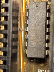
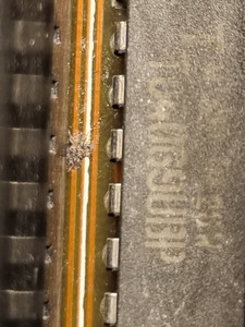
That hotspot could also have been attributed to some leftover flux sitting just under the pins for IRQ 14 and 15. Judging by the offset in the FLIR picture that would put the hotspot at these pins. It is somewhat conductive, once I cleaned it up properly the hotspot was gone. Judging by the heat scale/legend - that spot was somewhat warmer than the surroundings - but probably not something I could feel the difference of with my finger.
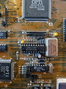
What I still find odd is that both IRQ 14 and 15 are inverted from the 82C822 - but it is only for IRQ 14 there is a pull-down on the input? I would expect the same also for IRQ 15?
Well the ATX-to-AT adapter was a complete let-down. I confirmed that all the voltages were OK on the adapter side, but with that option I do not get any POST code at all. Most likely it gives unstable voltages just after flicking the PS_ON# switch. Not even after trying to press reset a couple of times. It was just not meant to be 😀
Ok back to surgery then, first step - go over all the pads on the 82C206 with some nice flux and 63/37 solder. This would also help the melting temperature just a tiny bit (even though this board definitely already have leaded solder from factory).
Any chance that the psu isn’t supplying -5v and the board needs that? Sorry if this has been addressed, just a thought. (Long thread)
You are probably right, this board may very well require -5V. Took out an early ATX PSU I have which provides -5V rail and this one works with the ATX-to-AT adapter.
I don’t think that’s worth pulling the slot. But I’m not there. Looks like a fine tip can get to it. Scrape it, flux it and solder it. But you’re there and can see it better. Maybe you dissagree. I’d rather burn the slot than risk the board pulling the slot.
I found aluminum tape helps protect the slots when I have done work near them
I use aluminum tape - the kind sold at hardware stores for insulating air conditioning ducts - on slots and other components when I work near them. It's thicker than regular aluminum foil, plus it sticks in place where you put it so it won't move if you breathe too hard on it.
I/O, I/O,
It's off to disk I go,
With a bit and a byte
And a read and a write,
I/O, I/O
Well just when I thought I had explored it all, I stumbled upon this 😀
I agree with the common consensus from you guys with more soldering experience than me, I think I have the soldering tip for the job, but it sure will require some magnifying glasses and a steady hand! I will give it some flux and heat first and then go over with IPA again to see what's going on. It looks like there is a tiny trace just underneath the white mask line, which I do believe is burnt.
I have the very same cheap aluminum tape at disposal, I have also used it before as heatshield around BGAs when reflowing. I will use that to protect the site, thanks!
Would it be easier to remove the 4096 and get a better angle to see whether anything goes under the ISA slot. It looks like the signal trace from the nearby ISA pin is on the other side of the board, so if it has affected any traces it's probably only the ones you can see. I guess it's only surface muck anyway. Maybe your board had spiders?
Would it be easier to remove the 4096 and get a better angle to see whether anything goes under the ISA slot. It looks like the signal trace from the nearby ISA pin is on the other side of the board, so if it has affected any traces it's probably only the ones you can see. I guess it's only surface muck anyway. Maybe your board had spiders?
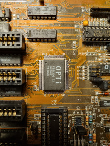
Plus we know (or are at least pretty certain) that the CMOS parts of the 206 are working. So it may not be the problem. rasz_pl has been working through the stage 0B parts of the BIOS, but it looks like a pretty chunky section setting up many things, including PCI stuff. So it could be the 822 VLB->PCI bridge is the problem.
At least 206 chips aren't too difficult to get hold of. I haven't even looked up the other chipset chips.
OTOH, looking at the mrbios listing of POST stages, all the interrupt testing comes later (stages 15-18). I don't see at what stage interrupts are actually enabled.
Interrupt vectors are loaded at 0A:
1.Initialize the first 32 interrupt vectors with corresponding interrupt handlers
Initialize INT No from 33120 with Dummy (Spurious) interrupt handler
2.Issue CPUID instruction to identify CPU type
actually is
1.Initialize the first 32 interrupt vectors with corresponding interrupt handlers
Initialize INT No from 33-120 with Dummy (Spurious) interrupt handler
-120 vectors (https://wiki.osdev.org/Interrupt_Vector_Table) are set to dummy 'iret'
-then first 32 vectors are set to actual handlers
-making double sure vector 32 is set to F000:0000 for some reason even tho there is no code there? please correct me on that (code at F0838)
-8 more vectors for Slave 8259
-then for some reason zeroes 8 more vectors 96-104
-checks if the processor can identify as "GenuineIntel", sets CMOS 0Fh bit 00100000b if it is
-write BDh to CMOS 3Dh if the CPU CPUID says "WB cache DX2"???? again please correct me on that (code at F7DF4)
and thats it, 8259 are not configured here. Looking at Award codes we should either look into:
C0
1.Turn off OEM specific cache, shadow
2.Initialize standard devices with default values:
DMA controller (8237)
Programmable Interrupt Controller (8259)
Programmable Interval Timer (8254)
RTC chip
or according to other table:
C0 Turn Off Chipset Cache; OEM specific cache control
03 Initialise Chips; Disable NMI/PIE/UEL/SQWV; video; parity checking; DMA; reset maths coprocessor. Clear all page registers and CMOS shutdown byte. Initialise timer 0 1 and 2 including set EISA timer to a known state. Initialise DMA controllers 0 and 1; interrupt controllers 0 and 1 and EISA extended registers.
In our bios C0 seemingly does only stuff to 82C822 bridge registers
-PCI Bridge Enable: 0 = Disable
-VGA Palette Snooping at ISA Bus (Address Decoded 3C6h-3C9h Write Cycle): 0= Disable
-some accesses I dont understand at F886C because they would only make sense if code was setting CX=2, that would address main chipset Cache Control Register 1 and all the subsequent registers to disable cache, but instead Bios Author here sets CL=2 meaning we are still talking to 82C822 ??? except bios is trying to write to READ ONLY registers and it makes no sense. Have I just found a BIOS bug or more likely didnt understand something again? 😀
-finally turns off Shadowed RAM for FOOOOh-FFFFFh. why is ram shadowing handled by 82C822 bridge I dont understand 🙁 datasheet says
"The 82C822 includes registers to determine shadow memory space, hole locations and sizes to allow the 82C822 to determine which memory space should be local and which is located on the ISA bus."
Now the thing is, ISA bus only supports edge interrupts, and 8259A are setup for edge, so even if you have stuck interrupt 14 it wouldnt trigger. Besides while I havent checked this thoroughly I think bios is enabling interrupts very late in POST_C, and up to that point they are disabled.
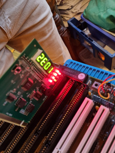
Aaanyway. Here is rather hilariously badly patched bios that will display on the POST card first 16 raw CMOS values, basically clock, when pressing ~1234567890-=<backspace>Tab keys. Every key is one value from 0 to 15. This way you will immediately see RTC running (offset 0 is seconds)
rasz_plwrote on 2022-02-09, 03:25:Interrupt vectors are loaded at 0A:
1.Initialize the first 32 interrupt vectors with corresponding interrupt handlers
Initialize […] Show full quote
OTOH, looking at the mrbios listing of POST stages, all the interrupt testing comes later (stages 15-18). I don't see at what stage interrupts are actually enabled.
Interrupt vectors are loaded at 0A:
1.Initialize the first 32 interrupt vectors with corresponding interrupt handlers
Initialize INT No from 33120 with Dummy (Spurious) interrupt handler
2.Issue CPUID instruction to identify CPU type
actually is
1.Initialize the first 32 interrupt vectors with corresponding interrupt handlers
Initialize INT No from 33-120 with Dummy (Spurious) interrupt handler
-120 vectors (https://wiki.osdev.org/Interrupt_Vector_Table) are set to dummy 'iret'
-then first 32 vectors are set to actual handlers
-making double sure vector 32 is set to F000:0000 for some reason even tho there is no code there? please correct me on that (code at F0838)
-8 more vectors for Slave 8259
-then for some reason zeroes 8 more vectors 96-104
-checks if the processor can identify as "GenuineIntel", sets CMOS 0Fh bit 00100000b if it is
-write BDh to CMOS 3Dh if the CPU CPUID says "WB cache DX2"???? again please correct me on that (code at F7DF4)
and thats it, 8259 are not configured here. Looking at Award codes we should either look into:
C0
1.Turn off OEM specific cache, shadow
2.Initialize standard devices with default values:
DMA controller (8237)
Programmable Interrupt Controller (8259)
Programmable Interval Timer (8254)
RTC chip
or according to other table:
C0 Turn Off Chipset Cache; OEM specific cache control
03 Initialise Chips; Disable NMI/PIE/UEL/SQWV; video; parity checking; DMA; reset maths coprocessor. Clear all page registers and CMOS shutdown byte. Initialise timer 0 1 and 2 including set EISA timer to a known state. Initialise DMA controllers 0 and 1; interrupt controllers 0 and 1 and EISA extended registers.
In our bios C0 seemingly does only stuff to 82C822 bridge registers
-PCI Bridge Enable: 0 = Disable
-VGA Palette Snooping at ISA Bus (Address Decoded 3C6h-3C9h Write Cycle): 0= Disable
-some accesses I dont understand at F886C because they would only make sense if code was setting CX=2, that would address main chipset Cache Control Register 1 and all the subsequent registers to disable cache, but instead Bios Author here sets CL=2 meaning we are still talking to 82C822 ??? except bios is trying to write to READ ONLY registers and it makes no sense. Have I just found a BIOS bug or more likely didnt understand something again? 😀
-finally turns off Shadowed RAM for FOOOOh-FFFFFh. why is ram shadowing handled by 82C822 bridge I dont understand 🙁 datasheet says
"The 82C822 includes registers to determine shadow memory space, hole locations and sizes to allow the 82C822 to determine which memory space should be local and which is located on the ISA bus."
Now the thing is, ISA bus only supports edge interrupts, and 8259A are setup for edge, so even if you have stuck interrupt 14 it wouldnt trigger. Besides while I havent checked this thoroughly I think bios is enabling interrupts very late in POST_C, and up to that point they are disabled.
Aaanyway. Here is rather hilariously badly patched bios that will display on the POST card first 16 raw CMOS values, basically clock, when pressing ~1234567890-=<backspace>Tab keys. Every key is one value from 0 to 15. This way you will immediately see RTC running (offset 0 is seconds)
Just a thought, could it be that some of the chipset wants a 33 MHz CLK instead of 66 FSB CLK? For example the 82C822 VLB-to-PCI bridge. Remember when we embarked upon this journey and the oscillator socket that was unpopulated? We were running a bit of a guessing game here whether this should use 33 or 66 MHz oscillator.
From what I can trace, the FSB CLK to CPU will run directly from the Chrontel 9007 regardless. Whereas jumper JP13 sets whether the same CLK (from Chrontel 9007) should be used as main system clock, or the "external" oscillator source. In fact in the condition the board was in when I got it; the jumper position was indeed in the position using the "external" oscillator source - just that there was no oscillator there 😀 In this position (and without oscillator in the socket, it will not give any POST code), with the oscillator in place then either jumper position "works".
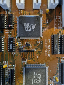
I would expect that the 571/572 hosts a 1/2 CLK divider and feeds that to the 822, but I'm not sure. We do at least have the datasheet for the 82C822, so possibly we can trace it backwards from there...
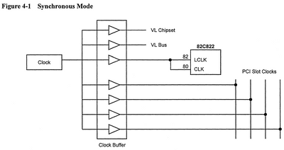
The 82C822 runs in "synchronous mode" so it will probably not be happy with 66 MHz.
Also what is the purpose of JP32 and JP34 sitting in-between 571 and 822 🤔
Pin 2 on 82C571 goes to Chrontel 9007, also known as ECLK (Early clock) ? This one does not pass the clock buffer. It does not show continuity with the 14.318 MHz reference clock either.
Pin 159 on 82C571 goes to R24, which in turn goes to JP13 - setting the oscillator source - both sources go via the 74ABT245N clock buffer.
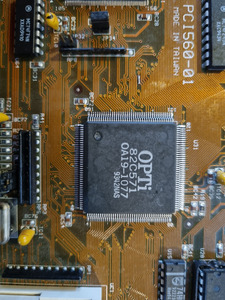
Pin 150 from 82C571 goes to pin 80, 82 and 89 on the 82C822, which implies synchronous mode since pin 80 and 82 are same. However, then pin 89 should not have been connected as well?
EDIT: pin 81 (not pin 80 and 82, tricked myself by looking at the datasheet) and pin 89 on the 82C822 is tied to GND! So is pin 150 on the 82C571. So from where would the 82C822 get LCLK (pin 82) and CLK (pin 80) ? Definitely synchronous mode then, just need to find the CLK source for the same:
LCLK, pin 159, I/O Local Bus Clock: This clock is used by local bus devices. Depending upon strapping of the Xd 1 pin at power-on reset, this can be either an input or output. LCLK =
CLK/2.
Last edited by LocalBus on 2022-02-09, 12:47. Edited 1 time in total.
Interesting idea. Looking back, I think the main Chrontel output is duplicated, with one branch going somewhere under the 571. The other branch goes to JP13, along with (probably) the output from the oscillator, JP13 selects which drives the middle pin. That middle pin directly drives the 572, and has two copies made, one which goes under the 571 and the other toward the Socket 4 (and I assume it then goes on the Socket 5). So the Chrontel seems to always drive the 571, and everything else can switch between the external oscillator or the Chrontel. I don't know where the PCI clock comes in from, but that has 4 copies made that go up to the slots.
Could try slowing the chrontel down. I never did find a 9007 datasheet. But the frequency outputs in that paper I found for the 9007 match the frequencies for the 9008D. So it's possible that the 9007E matches the 9008E. In which case it looks like JP28 is Fs0 (1-2), FS1 (3-4), FS2 (5-6), SD (7-8). The Slow Down (SD) input selects a slower speed when it is pulled low. All the inputs have internal pull ups, so I assume the jumper pull the line low when fitted. So the frequency table would be:
I don't know how low your CPU will clock, but maybe try 1-2,5-6 to select 40MHz?
[a datasheet for some Pentium processors suggests that the bus speed can go down to half. So, e.g., I think a P90 expecting a 60MHz bus should work as a P45 on a 30MHz bus.]
Last edited by snufkin on 2022-02-09, 14:29. Edited 1 time in total.