First post, by Paul_V

- Rank
- Newbie
Greeting to all forum members and fellow retro gamers,
I decided to create a post about Advantech PCM-3343 PC104 motherboard to share some info and hopefully, get some help regarding it's bios.
Some months ago, I got my hands on a pair of PCM-3343 motherboards, which I decided to test as a retro gaming rig.
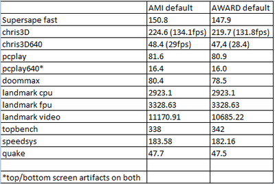
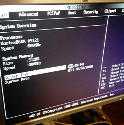
It has a Vortex86DX cpu, SMI712GF4 videochip and runs AWARD 6.00PG BIOS
While the BIOS has a neat ability to choose the CPU divider (from x1 to x32, as on most Vortex86DX boards), it does not have the ability to disable L1\L2 caches.
None of the utilities I've used are able to work with Vortex86DX cache correctly, or even detect it.
Datasheet on the CPU metions only regulating CPU speed (by adjusting 0A register, which I tested sucessfully)
The first thing I've tried - enabling the hidden options in BIOS, but that didn't work. Disabling cache does nothing, I assume manufacturer just didn't add the code for it.
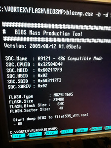
Moreover, I almost bricked a mobo - DONT USE THE "BIOS FLASH 1.1" UTILITY LISTED ON ADVANTECH SITE FOR PCM-3343 !, use BIOS F12 option (Flash from USB), or the utility for PCM-6743\9343 (VortexDX based)
The utility listed for pcm-3343 is for another model, it will detect the chip and backup it, but it flashes the chip incorrectly. After the first attempt you will not notice any changes, on the second attemp the utility will break the bios ability to boot from any device. The only thing that helped me - using a cheap USB-to-CF adapter, formatting CF card to FAT32, putting original bios file on it (rename it to update.bin), and the flash it using F12 option (none of the other usb sticks I had worked)
Now for the question itself:
This mobo does not have an external BIOS chip. Only one integrated in Vortex86DX itsef. So bricking this particular mobo is super easy.
It has a JTAG port, which can be used to flash the BIOS. The only information I could dig is that the chip can be flashed using a parralel port jtag cable (xilinx\wiggler) and a "JFlash" utility.
The only thing regarding "JFlash" utility i could find is "Flash Memory Programmer for the SA-1110 Microprocessor Development Board". But it's an ARM based board. As far as I know, I can't just connect to JTAG and flash a chip. I need something like BDSL file, which will tell the programmer how to operate with CPU and scan it's chain. I could not find any more info regarding which software I should use and how.
Has somebody succesfully used JTAG on this boards?
Why do I need it:
1) For obvious reasions of being able to unbrick the mobo. (While it is possible to solder external SPI on the mobo, I don't know the registers which will tell the CPU to use external bios, nor yet the understanding of missing components on circuit and how to implement it)
2) I have an idea to attempt to cross-flash the AMI BIOS from the other manufacturer mobo, which use the same components (CPU+video). As Vortex86DX is basically a SoC, it should theoretically work. But I need JTAG to be able to revert thr BIOS should this fail.
Any info or help is much appreciated, I'll try to post any updates on the progress should anyone stumble upn this mobo's.