1 x PLCC-68 / 2 x PGA132 / 5 x Skt 3 / 9 x Skt 7 / 12 x SS7 / 1 x Skt 8 / 14 x Slot 1 / 5 x Slot A
5 x Skt 370 / 8 x Skt A / 2 x Skt 478 / 2 x Skt 754 / 3 x Skt 939 / 7 x LGA775 / 1 x LGA1155
Current PC: Ryzen 7 5800X3D
Backup PC: Core i7 7700k
Pardon my late arrival to this thread, but I couldn't help but wonder if anyone knows the rationale for disabling half the cache on the K6-2+ chips? With the Pentium Pro chips, I'm pretty sure that the difference between 256k, 512k, and 1024K was the presence of less cache, and consequently less manufacturing cost. For the K6 chips, was it just that the cost difference between 128k and 256k was less than the cost to have a dye with two cache sizes?
Plan your life wisely, you'll be dead before you know it.
Pardon my late arrival to this thread, but I couldn't help but wonder if anyone knows the rationale for disabling half the cache on the K6-2+ chips? With the Pentium Pro chips, I'm pretty sure that the difference between 256k, 512k, and 1024K was the presence of less cache, and consequently less manufacturing cost. For the K6 chips, was it just that the cost difference between 128k and 256k was less than the cost to have a dye with two cache sizes?
The pentium pro used separate dies for the cache and core.
I assume the reason for the k6 2+\3+ was partially to increase yields by pushing ones with partially damaged cache to market with part disabled, as we have seen this is the case on some, but as well to also give several options as to capture more price points. Kinda like pentium vs celeron. We have obviously seen that there were many with good cache that also got the cut.
Then a full story:
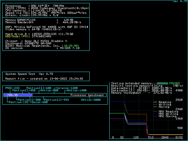
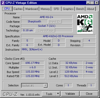
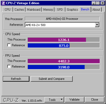
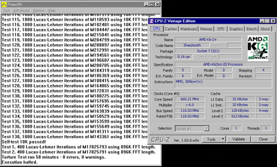
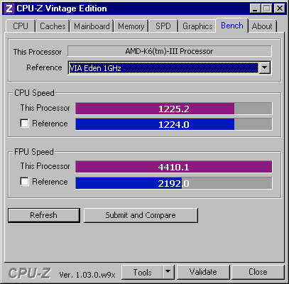
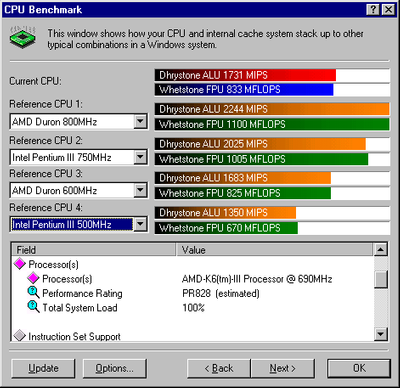
About a month ago, a batch of three AMD K6-2+ 570 MHz (570ACZ) from a well known seller finally arrived. I prepared my trusty Gigabyte GA-5AA (cache stable at 115 MHz FSB), nice cooler with a copper core and began. First I quickly confirmed that each is capable of 600 MHz @ 2.0V - this was no problem. Then I set 2.2V to check maximal OC potential. One of the CPUs (#3) was able to load Windows at 690 MHz and seemed stable:
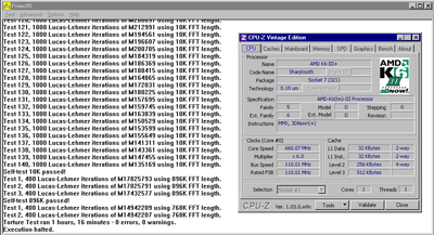
Unfortunately Prime95 quickly showed an instability. At that point I said "OK, let's see, what 2.4V can do!". With this voltage I didn't want to torture this CPU in Prime, so I just tried how far can I go. At 720 MHz (6x120 with disabled L3), computer went through POST, but even DOS applications were crashing. As a final resort I tried combination 700 MHz (5x140 with disabled L3) which seemed stable in DOS and this is where I took this:
But Windows was a no-go. Funny thing is, I confirmed later that 140 MHz FSB is unstable even without cache, so for 700 MHz Windows "experience" I would need a better board.
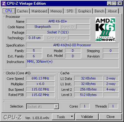
Finally I wanted to check how far can I go at a standard 2.0V. To my great surprise it was 660 MHz (6x110):
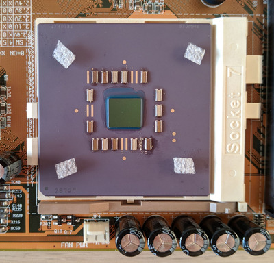
Yesterday, I finally decided to go with the mod for the best CPU (#3) in the batch. After de-lidding, some cleaning (btw. plastic eraser is great for scrubbing the remnants of TIM from CPU) and de/re-soldering of the link (here I am not sure if it's a 0 Ohm link or a capacitor because my measurement showed 32 pF of capacity) the deed was finally done (sorry, no time for cleaning 😀):
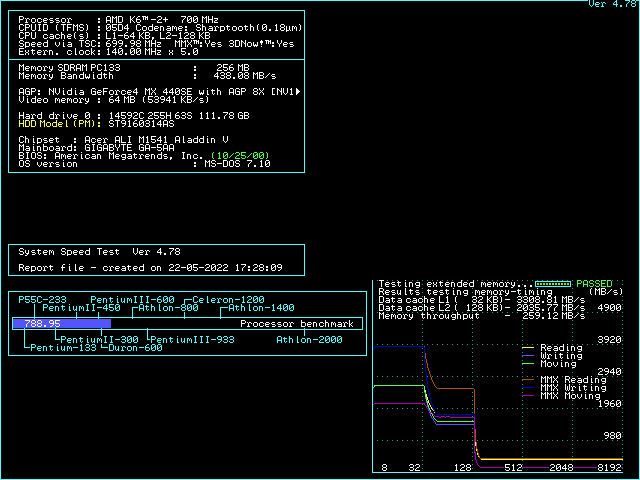
I didn't want to waste time with re-attaching of heatspreader so I went ahead carefully with on die cooling. During the first POST, I was holding my breath, but there were no cache errors! Then I used memtest as per guide to test the cache properly and everything was OK. After that I basically confirmed what I have tested before: 700 MHz @ 2.4V is still highly unstable (as I wrote, here I would blame the board), 690 MHz @ 2.2V is still Prime95 unstable, but more importantly 660 MHz @ 2.0V is still stable. I went as far as to lower the voltage to 1.9V and it still managed to do over an hour of Prime95 without any issue:
Sphere's been selling them for a while (I want to say a few months?)
See my graphics card database at www.gpuzoo.com
Constantly being worked on. Feel free to message me with any corrections or details of cards you would like me to research and add.
I recorded this almost a month ago, finally managed to upload the video today: https://www.youtube.com/watch?v=5Aw2U_BZnSk
It's a guide with the method I'm using for modding the K6-2+ to a K6-3+, maybe it will help others.
Probably mine? I wrote about it 3 months ago on this exact thread (see quote above), but I'm guessing you missed it. 😀
1 x PLCC-68 / 2 x PGA132 / 5 x Skt 3 / 9 x Skt 7 / 12 x SS7 / 1 x Skt 8 / 14 x Slot 1 / 5 x Slot A
5 x Skt 370 / 8 x Skt A / 2 x Skt 478 / 2 x Skt 754 / 3 x Skt 939 / 7 x LGA775 / 1 x LGA1155
Current PC: Ryzen 7 5800X3D
Backup PC: Core i7 7700k
I recorded this almost a month ago, finally managed to upload the video today: https://www.youtube.com/watch?v=5Aw2U_BZnSk
It's a guide with the method I'm using for modding the K6-2+ to a K6-3+, maybe it will help others.
Probably mine? I wrote about it 3 months ago on this exact thread (see quote above), but I'm guessing you missed it. 😀
If
I noticed it, I forgot. 🤣.
I’m going to add it to the guide on page 13 thank you 😀
I’m going to add it to the guide on page 13 thank you 😀
Great, you're welcome! 😀
1 x PLCC-68 / 2 x PGA132 / 5 x Skt 3 / 9 x Skt 7 / 12 x SS7 / 1 x Skt 8 / 14 x Slot 1 / 5 x Slot A
5 x Skt 370 / 8 x Skt A / 2 x Skt 478 / 2 x Skt 754 / 3 x Skt 939 / 7 x LGA775 / 1 x LGA1155
Current PC: Ryzen 7 5800X3D
Backup PC: Core i7 7700k