VOGONS


New clock gen for tyan s1564d (Research)

Topic actions

Reply 60 of 105, by stamasd

User metadata
Rank l33t
Rank
l33t

Well they're limited by other things too: chipsets, integrated peripherals like IDE/floppy, bus buffers etc which may or may not like the higher speeds.

I/O, I/O,
It's off to disk I go,
With a bit and a byte
And a read and a write,
I/O, I/O

Reply 61 of 105, by Sphere478

User metadata
Rank l33t++
Rank
l33t++
stamasd wrote on 2022-02-16, 03:27:

Well they're limited by other things too: chipsets, integrated peripherals like IDE/floppy, bus buffers etc which may or may not like the higher speeds.

Of course. On some applications async may be a possibility. (I don’t think the tyan will accept that though)

Sphere's PCB projects.
-
Sphere’s socket 5/7 cpu collection.
-
SUCCESSFUL K6-2+ to K6-3+ Full Cache Enable Mod
-
Tyan S1564S to S1564D single to dual processor conversion (also s1563 and s1562)

Reply 62 of 105, by Sphere478

User metadata
Rank l33t++
Rank
l33t++
snufkin wrote on 2022-02-11, 11:49:
Sphere478 wrote on 2022-02-11, 00:27:

3.3v to ground from cap pad closest to chip

That's good. Assuming that all the Vin pins are the same voltage (they've got the same resistance to ground, so I think it's likely) then I think that means level shifters aren't needed. Last thing, would you mind measuring the voltage on both sides of R48. I'm curious whether the inputs to the clock gen are 5V tolerant, or if they clamp the input to 3.3V.

R48
I got 4.7v on both sides which is what my atx2at shows on the 5v rail

Sorry it took a while to get this to ya. Apologies.

Sphere's PCB projects.
-
Sphere’s socket 5/7 cpu collection.
-
SUCCESSFUL K6-2+ to K6-3+ Full Cache Enable Mod
-
Tyan S1564S to S1564D single to dual processor conversion (also s1563 and s1562)

Reply 63 of 105, by snufkin

User metadata
Rank Oldbie
Rank
Oldbie
Sphere478 wrote on 2022-02-18, 05:16:
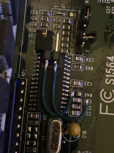
R48
I got 4.7v on both sides which is what my atx2at shows on the 5v rail

Sorry it took a while to get this to ya. Apologies.

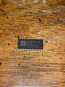
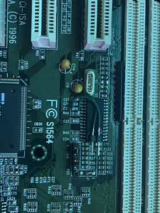
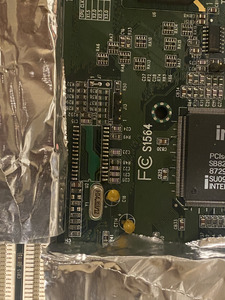
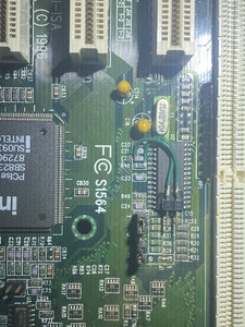
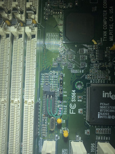
No worries, but that 4.7/5V bothers me a bit. We're fairly sure, based on the voltage you measured on C20 (goes to pin 1) and the resistance to ground of all the Vcc pins, that all the chip power pins are at 3.3V. I'm pretty sure that all the clock gen chip datasheets I've seen have a maximum input voltage for logic inputs of Vcc+0.5V. So in this case the input voltages shouldn't be higher than 3.8V. I don't know why they've pulled it to 5V. Given it hasn't broken then the standard clock gen chips must be fine with 5V on the inputs and the datasheets are just using the standard absolute maximums.

More modern chips are probably less tolerant of that though. So to be on the safe side, any adapter will probably want to clamp the OE and FSel pins to maximum 3.3V. Not certain how best to do that. Series resistor and then a low voltage Schottky diode to Vcc, or 3.3V zener to Ground, maybe? Or just not use them at all, though I had thought it would be nice to still be able to use the existing jumpers to select frequencies.

Thought just occurred to me, which I don't know that answer to, about power sequencing. Power comes up and the board is initially held in reset. Various things start to happen, including the board getting a Power Good signal from somewhere (PSU, on board voltage monitoring?) and oscillators start oscillating. I think I remember reading that some CPUs (I think 386 / 486) need a stable clock for a number of cycles before reset is released. It's possible that the board doesn't check the clock and just assumes that it will have become stable some fixed time after power good has been signaled, and so it releases reset a fixed time (time to stable oscillator + CPU wait) after power good.

If it does just wait a fixed time then there could be a problem with using a programmable clock gen. It's going to take a bit of time to program the chip after power comes up, by which time maybe the board will already have released reset. If it does, then the CPU won't have the pre-reset release cycles.

Might not be a problem. I could be misremembering about the CPU clocking requirements, or the programming would be fast enough to not matter, or (even if I have remembered correctly) the CPU is actually fine. If it is a problem then the new clock gen could be wired in to the board reset, so that it can hold on to reset until it's ready. But that starts to get away from it being a drop in replacement.

Reply 64 of 105, by stamasd

User metadata
Rank l33t
Rank
l33t

I think that reset release can be worked in the Arduino code. I can probably measure how long it takes from the Arduino/SI5351 power up until a stable signal is present at the output, work out a delay loop and use one of the many unused pins on the Arduino as a reset release pin with an appropriate delay.

Whatever that delay is, it would be less than 1 second based on the timing I see on the waveform output. At a (subjective) second after power up, there is already a stable clock signal. So if anything, a 1s delay till the microcontroller releases the CPU reset should be enough. And Arduino boots in a few miliseconds because it has only a very minimal bootloader which immediately starts executing the programmed code on the bare metal, there is no OS to load. And a few miliseconds from that to the programming of the PLL which is done over the relatively slow I2C interface, and yet it only takes a few 8-bit packets to do the programming. The reset release can be then programmed to happen a certain amount of time _after_ that programming is already finished.

Also here's a quick overview of all the FSBs which can be easily programmed using only reliable integer math

si5351: using only integer mode
freq=25MHz*mult/div/R
mult=15..90
div=4,6 or 8
R=1..128

50MHz: 25*16/8=50

55MHz: 25*18/8=56.25

60MHz: 25*19/8=59.375
25*15/6=62.5

66MHz: 25*16/6=66.66

70MHz: 25*22/8=68.75
25*17/6=70.833
25*23/8=71.875

75MHz: 25*24/8=75

78MHz: 25*25/8=78.125

81MHz: 25*26/8=81.25

83MHz: 25*20/6=83.33

87MHz: 25*28/8=87.5

90MHz: 25*29/8=90.625

95MHz: 25*30/8=93.75
25*23/6=95.833
25*31/8=96.875

100MHz: 25*16/4=100

106MHz: 25*17/4=106.25

112MHz: 25*18/4=112.5

120MHz: 25*19/4=118.75
25*29/6=120.833

125MHz: 25*20/4=125

133MHz: 25*32/6=133.33

none of the above needs any R; for the 1/2 clock signal use a R=2 on the same PLL

I am waiting for a better oscilloscope before I get anything else done; I ordered it but it'll probably take a week or two to get here.
The plan would be to have the clockgen come up at power on with a "safe" FSB, probably 66MHz; after that the FSB would be immediately selectable among the values above with a rotary encoder, and displayed on a little OLED panel.

I/O, I/O,
It's off to disk I go,
With a bit and a byte
And a read and a write,
I/O, I/O

Reply 65 of 105, by Sphere478

User metadata
Rank l33t++
Rank
l33t++

Okay…. Here we go..

Gotta re read the thread and re familiarize myself.

Did we ever make a diagram for how I’m supposed to configure this?

Attachments

Sphere's PCB projects.
-
Sphere’s socket 5/7 cpu collection.
-
SUCCESSFUL K6-2+ to K6-3+ Full Cache Enable Mod
-
Tyan S1564S to S1564D single to dual processor conversion (also s1563 and s1562)

Reply 66 of 105, by Sphere478

User metadata
Rank l33t++
Rank
l33t++

Okay… double check me here

Did I do it right?

Attachments

Sphere's PCB projects.
-
Sphere’s socket 5/7 cpu collection.
-
SUCCESSFUL K6-2+ to K6-3+ Full Cache Enable Mod
-
Tyan S1564S to S1564D single to dual processor conversion (also s1563 and s1562)

Reply 67 of 105, by Sphere478

User metadata
Rank l33t++
Rank
l33t++

Did a little cleanup.

Hoping for some confirmation before I give it power.

Attachments

  • image.jpg
    Filename
    image.jpg
    File size
    1.75 MiB
    Views
    872 views
    File license
    Public domain

Sphere's PCB projects.
-
Sphere’s socket 5/7 cpu collection.
-
SUCCESSFUL K6-2+ to K6-3+ Full Cache Enable Mod
-
Tyan S1564S to S1564D single to dual processor conversion (also s1563 and s1562)

Reply 68 of 105, by Sphere478

User metadata
Rank l33t++
Rank
l33t++

Well, I went ahead and tried it using the atx2at device. Doesn’t seem to be drawing any kind of abnormal current but it’s also not working.

The diag card is stuck on c01 or something rather and the display digits are glitching.

Thoughts?

Sphere's PCB projects.
-
Sphere’s socket 5/7 cpu collection.
-
SUCCESSFUL K6-2+ to K6-3+ Full Cache Enable Mod
-
Tyan S1564S to S1564D single to dual processor conversion (also s1563 and s1562)

Reply 69 of 105, by Sphere478

User metadata
Rank l33t++
Rank
l33t++

Poke

Sphere's PCB projects.
-
Sphere’s socket 5/7 cpu collection.
-
SUCCESSFUL K6-2+ to K6-3+ Full Cache Enable Mod
-
Tyan S1564S to S1564D single to dual processor conversion (also s1563 and s1562)

Reply 71 of 105, by Sphere478

User metadata
Rank l33t++
Rank
l33t++
rasz_pl wrote on 2022-02-25, 22:28:

do you have any any of measuring frequencies?

I can see if my fluke can do it.

Sphere's PCB projects.
-
Sphere’s socket 5/7 cpu collection.
-
SUCCESSFUL K6-2+ to K6-3+ Full Cache Enable Mod
-
Tyan S1564S to S1564D single to dual processor conversion (also s1563 and s1562)

Reply 72 of 105, by snufkin

User metadata
Rank Oldbie
Rank
Oldbie

Looks right. Hmm. Things I'd check/change:
-C22 is part of the crystal oscillator circuit (I should have guessed that, but can now see the tracks under the clock gen). I know you've soldered to the ground side, but I always get worried around crystals so I'd probably try and find a different ground to use as the pull down for pin 5.
-Remove R48 entirely. I'm not happy about it pulling pin 5 to 5V when based on your measurements the rest of the chip is at 3.3V. 5V is above the absolute maximum (Vdd+0.5), and whilst it worked on the previous chip, it may damage this one. The chip has internal pull ups, so shouldn't need an external one.
-Check there's about 100 ohm resistance (R31) from pin 27 (reference 14.318MHz output) to that 0ohm link you moved (side furthest from the RAM slots).
-All jumpers off should be CPU clock of 55MHz, so that should be ok.
-J13 1-2 is FS1 and 3-4 is FS0. If you short 3-4 then the CPU output should either be 60 or 61.6MHz depending on the Turbo (pin 5) input.
-It'll be a faff, but might be worth putting the original one back and seeing if it still works with the 0 ohm link moved (double checking that the KBC is ok at 14MHz).

It is possible that the chip is duff, but difficult to check that without a fast scope.

Reply 73 of 105, by Sphere478

User metadata
Rank l33t++
Rank
l33t++
snufkin wrote on 2022-02-25, 22:59:
Looks right. Hmm. Things I'd check/change: -C22 is part of the crystal oscillator circuit (I should have guessed that, but can […]
Show full quote

Looks right. Hmm. Things I'd check/change:
-C22 is part of the crystal oscillator circuit (I should have guessed that, but can now see the tracks under the clock gen). I know you've soldered to the ground side, but I always get worried around crystals so I'd probably try and find a different ground to use as the pull down for pin 5.
-Remove R48 entirely. I'm not happy about it pulling pin 5 to 5V when based on your measurements the rest of the chip is at 3.3V. 5V is above the absolute maximum (Vdd+0.5), and whilst it worked on the previous chip, it may damage this one. The chip has internal pull ups, so shouldn't need an external one.
-Check there's about 100 ohm resistance (R31) from pin 27 (reference 14.318MHz output) to that 0ohm link you moved (side furthest from the RAM slots).
-All jumpers off should be CPU clock of 55MHz, so that should be ok.
-J13 1-2 is FS1 and 3-4 is FS0. If you short 3-4 then the CPU output should either be 60 or 61.6MHz depending on the Turbo (pin 5) input.
-It'll be a faff, but might be worth putting the original one back and seeing if it still works with the 0 ohm link moved (double checking that the KBC is ok at 14MHz).

It is possible that the chip is duff, but difficult to check that without a fast scope.

I removed r48 and lifted the ground wire off the capacitor all jumpers open

Still not working.

Gonna have to run soon, whatcha think?

Attachments

  • image.jpg
    Filename
    image.jpg
    File size
    1.7 MiB
    Views
    825 views
    File license
    Public domain
  • image.jpg
    Filename
    image.jpg
    File size
    947.81 KiB
    Views
    826 views
    File license
    Public domain

Sphere's PCB projects.
-
Sphere’s socket 5/7 cpu collection.
-
SUCCESSFUL K6-2+ to K6-3+ Full Cache Enable Mod
-
Tyan S1564S to S1564D single to dual processor conversion (also s1563 and s1562)

Reply 74 of 105, by Sphere478

User metadata
Rank l33t++
Rank
l33t++

I have 100 ohms between the second to last pin on ram side and the 0 ohm link I moved

Sphere's PCB projects.
-
Sphere’s socket 5/7 cpu collection.
-
SUCCESSFUL K6-2+ to K6-3+ Full Cache Enable Mod
-
Tyan S1564S to S1564D single to dual processor conversion (also s1563 and s1562)

Reply 75 of 105, by snufkin

User metadata
Rank Oldbie
Rank
Oldbie

This has some possible post code interpretation for Award BIOSes: http://mrbios.com/techsupport/award/postcodes.htm . I thought POST cards had the most recent completed test on the right and the current test on the left, so seems a bit odd to have it completed C1 and hanging on C0. Looks like the C tests are chipset related stuff (cache and RAM). At the moment, assuming the clock gen chip itself is ok, then I'd guess that either the KBC has problems at 14MHz or maybe there's more than just the keyboard that used the 12MHz output on the original chip, that went via that 0 ohm link, and if there is, that doesn't like 14MHz.

Reasonable high-res photos of the front and back might make it possible to trace where that signal goes.
[edit: oh, and just because I really am paranoid about crystals not starting up, remove that jumper wire on R48 as well. I can't believe it's a problem, but the insulation for the wire looks like it's resting on that capacitor, which might be a problem.

On the other hand, to get to displaying digits on the POST card suggests there's quite a lot working, which would mean the chip must be producing a working CPU clock of some sort.]

[2nd edit to fix broken link. On rasz_pl's point, with pin 5 left disconnected the J13 should work as on the original. So fitting both 1-2 and 3-4 should be 50MHz and is the slowest it goes. Fitting just 3-4 is probably safest since pin 5 only changes that from 60MHz to 61.6MHz, so a problem with pin 5 doesn't suddenly jump the CPU up to 83MHz.]

Last edited by snufkin on 2022-02-26, 00:45. Edited 1 time in total.

Reply 76 of 105, by rasz_pl

User metadata
Rank l33t
Rank
l33t

yes, c0c1 looks legit, cpu must be running at lest a little bit
remove ram and see if its the same code
I would also try different frequency jumper settings

Open Source AT&T Globalyst/NCR/FIC 486-GAC-2 proprietary Cache Module reproduction

Reply 77 of 105, by Sphere478

User metadata
Rank l33t++
Rank
l33t++
rasz_pl wrote on 2022-02-26, 00:29:

yes, c0c1 looks legit, cpu must be running at lest a little bit
remove ram and see if its the same code
I would also try different frequency jumper settings

It’ll be a bit before I’m in front of it again.

I tried a few different fsb settings when I first installed it but it made no difference. You can’t tell in the pic, but it glitches (some of the lights go out, and back on again)

Is there a way I can use two clock gens stacked on top of one another? Maybe the old one on top to make the 12mhz?

How far along are we on the other thing? The universal frequency generator thing.

Sphere's PCB projects.
-
Sphere’s socket 5/7 cpu collection.
-
SUCCESSFUL K6-2+ to K6-3+ Full Cache Enable Mod
-
Tyan S1564S to S1564D single to dual processor conversion (also s1563 and s1562)

Reply 78 of 105, by Sphere478

User metadata
Rank l33t++
Rank
l33t++

What if instead of moving the jumper, I lift the leg and run it over to the pad that it’s supposed to go to?

Sphere's PCB projects.
-
Sphere’s socket 5/7 cpu collection.
-
SUCCESSFUL K6-2+ to K6-3+ Full Cache Enable Mod
-
Tyan S1564S to S1564D single to dual processor conversion (also s1563 and s1562)

Reply 79 of 105, by snufkin

User metadata
Rank Oldbie
Rank
Oldbie
Sphere478 wrote on 2022-02-26, 05:31:

What if instead of moving the jumper, I lift the leg and run it over to the pad that it’s supposed to go to?

Not sure if that will change anything. The chip has 2 reference frequency outputs on pins 27 & 28. The one from 27 goes through R31, where it then splits with one branch heading back to where the 0 ohm link now is. If you were to lift pin 27 and connect it directly to the 0 ohm link then the only difference is that it bypasses the 100 ohm R31 resistor. That resistor is probably needed to terminate the clock net properly to stop ringing on the line.

Might be worth trying lifting pin 25. That's the one that's now a 48MHz output, and stops where the 0 ohm link used to be. Maybe that's causing some interference?