I have a fluke. Want me to measure some of the SMD components?
If electrical characteristics are not encoded on the cover, yes. 😉
But more interesting would be an electrical diagram of address line A19. For this purpose, you only have to search for those soldering points whose wire to
- CPU pin AK22
- L2 cache pin 52
- TagRAM pin 1
has an electrical resistance of 0-0.3 Ohm.
I would do it myself if I had a P5A but I never was so unlucky. 😉
Lotosdrachewrote on 2021-12-29, 11:35:And now you know why I'm so happy when looking at my GA-5AX Rev. 5.2 and said that I never had tough luck in finding a P5A for a […] Show full quote
And now you know why I'm so happy when looking at my GA-5AX Rev. 5.2 and said that I never had tough luck in finding a P5A for an acceptable price. 😉
Why?
1st. My GA-5AX has Rev H of Aladdin V chipset. So it supports internal TagRAM.
2nd. Gigabyte designed it very well so it supports K6-III+ and K6-2+ cpus without any performance loss and without the need of any hardware modifications. They even published an adapted BIOS.
3rd. Power supply seems to be very good. I could even run a Fire GL 8800 (=Radeon 8500) on it.
There is no P5A that combines these features.
Tom's Hardware once found it to be slow. However, adjust memory timings according to P5A settings and you get some extra speed!
I would be interested in some benchmarks of your board with modified bios vs a 1.04 p5a F north bridge🤔 (1.04 came with F sometimes right?)
The black resistor says 000 btw (the one you said was for power, the other one I assume is a cap it’s blank just tan in color) the cache size selector resistor also says 000 (the black one for 512 vs 1024k)
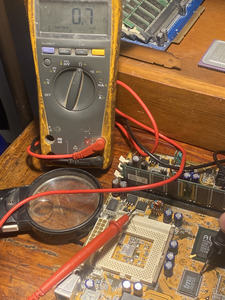
To measure I guess I would have to unsolder?
Benchmarks would really be interesting but they only make sense if everything else of the system (graphics card, sound card, driver versions, Windows installation...) is identical.
Board rev 1.04 comes with chipset revision E (mostly). Rev F may exist on P5A but I never saw it.
Yes, desoldering is necessary for measurement. The tan C50 should be a cap. That's why there is a C in front of the number. 😉
Have a look at Roman555's scheme here adapted for Asus P5A:
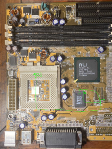
Now you have to find the gap(s) in address line A19 that corresponds to R171 of the diagram. It should be directly connected to L2 pin 52, CPU pin AK22, and Tag pin 1 as I showed you here. On Jetway 542C it's R304, on Gigabyte GA-5AX it's R46.
Last edited by Lotosdrache on 2022-01-13, 16:16. Edited 1 time in total.
Lotosdrachewrote on 2021-12-29, 14:35:Benchmarks would really be interesting but they only make sense if everything else of the system (graphics card, sound card, dri […] Show full quote
I would be interested in some benchmarks of your board with modified bios vs a 1.04 p5a F north bridge🤔 (1.04 came with F sometimes right?)
The black resistor says 000 btw (the one you said was for power, the other one I assume is a cap it’s blank just tan in color) the cache size selector resistor also says 000 (the black one for 512 vs 1024k)
To measure I guess I would have to unsolder?
Benchmarks would really be interesting but they only make sense if everything else of the system (graphics card, sound card, driver versions, Windows installation...) is identical.
Board rev 1.04 comes with chipset revision E (mostly). Rev F may exist on P5A but I never saw it.
Yes, desoldering is necessary for measurement. The tan C50 should be a cap. That's why there is a C in front of the number. 😉
Have a look at Roman555's scheme here adapted for Asus P5A:
ali-sram-upgrade.png
Now you have to find the gap(s) in address line A19 that corresponds to R171 of the diagram. It should be directly connected to L2 pin 52, CPU pin AK22, and Tag pin 1 as I showed you here. On Jetway 542C it's R304, on Gigabyte GA-5AX it's R46.
I’m following with the resistors and capacitors but you lost me on the address line. Going over it trying to understand gimme a second..
That looks fine!
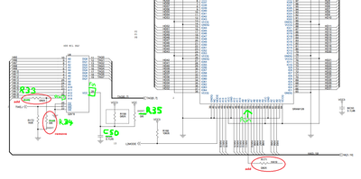
It means there will be a direct connection between CPU Pin AK22 (red) and TagRAM Pin 1 (black) as soon as you will have soldered a resistor at R33.
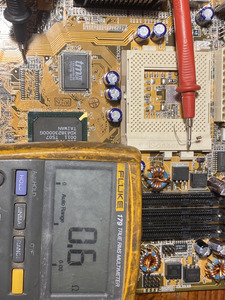
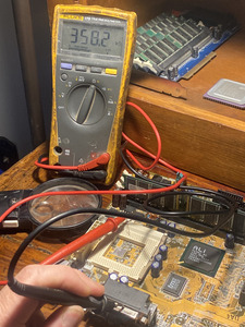
Don't worry about 0.6 Ohm. I made the experience that resistance increases with the length of the wire. It's just physics.
Now put your black test prod on Pin 52 of L2 cache and keep your red one where it is:
It's tricky but possible not to touch nearby pins of L2.
I guess there will be a high resistance indicating a cable interruption on address line A19. If not, you're lucky.
And then the other way round: Keep your black prod on R33 and put your red one on L2 pin 52.
That's possible and quite similar to my Jetway 542C.
So you can connect all three points, CPU pin AK22, L2 cache pin 52, and TagRAM pin 1, by just soldering one single resistor at position R33.
That's nice.
Now we need the value of this resistor. I guess it should be 0 Ohm but I'm not sure. @luckbob said he has got a 1 MiB P5A. Would be nice hearing him again. 😀
Is there any connection to L2 cache pin 40 or 41?
Last edited by Lotosdrache on 2021-12-30, 10:11. Edited 1 time in total.
Hence the electrical diagram of address line A19 on Asus P5A looks like this?
image.jpg
That's possible.
So you can connect all three points, CPU pin AK22, L2 cache pin 52, and TagRAM pin 1, by just soldering one single resistor at position R33.
That's nice.
Now we need the value of this resistor. I guess it should be 0 Ohm but I'm not sure. @luckbob said he has got a 1 MiB P5A. Would be nice hearing him again. 😀
I don't understand.
What do you mean? Can you draw the picture, please?
You showed that cpu AK22 is connected to the resistor side that's away from Tag.
Lotosdrachewrote on 2021-12-30, 10:18:I don't understand.
What do you mean? Can you draw the picture, please?
You showed that cpu AK22 is connected to the resistor si […] Show full quote
I don't understand.
What do you mean? Can you draw the picture, please?
You showed that cpu AK22 is connected to the resistor side that's away from Tag.
That would be interesting because on my Gigabyte GA-5AX there is an extra bridge to connect L2 pin 40 and on Jetway 542C L2 pin 40 is grounded. I'm not sure how to deal with this.
Lotosdrachewrote on 2021-12-30, 10:34:Like this?
image.jpg
That would be interesting because on my Gigabyte GA-5AX there is an extra bridge to connect L2 pin 40 and o […] Show full quote
Resistor pad closest to rear is connected to cpu pin and pin 40 on cache
Like this?
image.jpg
That would be interesting because on my Gigabyte GA-5AX there is an extra bridge to connect L2 pin 40 and on Jetway 542C L2 pin 40 is grounded. I'm not sure how to deal with this.
I’ve run into a roadblock for getting these chips.
I can find the cache chips but not the tag chip
They want 6$ a cache chip, initially I was gonna grab like 10 but at 6$ I’m like just give me 2
Then they are like: shipping is 50$ I’m like: use a envelope… anyway that went nowhere and I’m not paying 62$ for two measly chips.
Aren’t there pentium II/III cpus with these chips on them? I could just get one of those for like 10-15$ and harvest them? Edit: no go didn’t come large enough..
I would not recommend desoldering and re-soldering these 128-pin QFP chips. It´s a PITA to adjust all pins due to the very tiny pitch. There´s also a higher risk of overheating and ESD damage.
I would not recommend desoldering and re-soldering these 128-pin QFP chips. It´s a PITA to adjust all pins due to the very tiny pitch. There´s also a higher risk of overheating and ESD damage.
Torch to the back of the donor board and tweasers on the chip and it’s good to go 🤣.
Lotosdrachewrote on 2021-12-29, 11:35:1st. My GA-5AX has Rev H of Aladdin V chipset. So it supports internal TagRAM.
2nd. Gigabyte designed it very well so it support […] Show full quote
1st. My GA-5AX has Rev H of Aladdin V chipset. So it supports internal TagRAM.
2nd. Gigabyte designed it very well so it supports K6-III+ and K6-2+ cpus without any performance loss and without the need of any hardware modifications. They even published an adapted BIOS.
3rd. Power supply seems to be very good. I could even run a Fire GL 8800 (=Radeon 8500) on it.
There is no P5A that combines these features.
Gigabyte used linear regulator for VCC3, but they put a jumper near the DIP-switch which allows shorting ATX PS 3.3V and VCC3. Without it the regulator would get HOT (or even breakdown) with that kind of load. Radeon 8500 ~7A. LX8383A-00CP is rated max 7.5A. How are your jumpers positioned? Horizontally or vertically?
Asus used PWM controller for VDDIO with much better efficiency. Still, there is a not-assembled jumper pack to do the same thing (ATX PS 3.3 to VDDIO). Located between CPU and ATX-connector. Of course it will drop the default 3.5V IO to 3.3V. I have no experience is P5A stabile with 3.3 VDDIO. Anyway, the PWM controller design is good enough for everything I would use in socket 7 machine.
Don't get me wrong, I'm not saying P5A is better. It's just that both are great boards with their flaws (more on P5A 1.06).