VOGONS


Gigabyte GA-586HX (Rev. 1.53)

Topic actions

First post, by majestyk

User metadata
Rank Oldbie
Rank
Oldbie

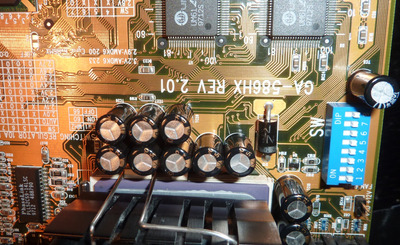
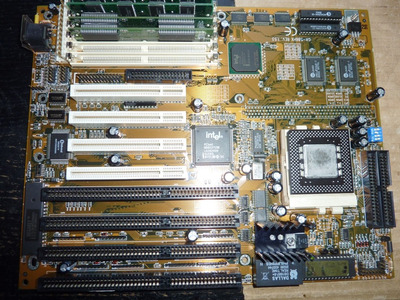
I recently found a GA-586HX (early revision 1.53) in very good condition. So I started experimenting with different CPUs.
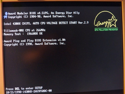
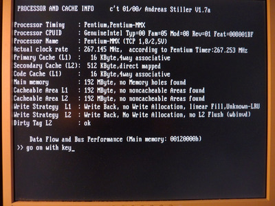
To get a Pentium MMX 233 running the latest BIOS (2.9) had to be installed. Then I did the "BF0 mod" to pull up the BF0 pin to Vcc when the DIP-switch is open.

ga5hx_bf0.JPG
Filename
ga5hx_bf0.JPG
File size
253.13 KiB
Views
1824 views
File license
Fair use/fair dealing exception

This worked well and the CPU is being identified by the BIOS correctly, the multiplier setting x 1.5 is interpreted as x 3.5 and the automatic voltage detection makes the VRM-transistor deliver 2.9 V core voltage.
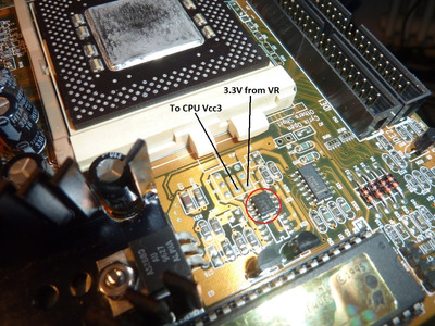
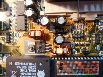
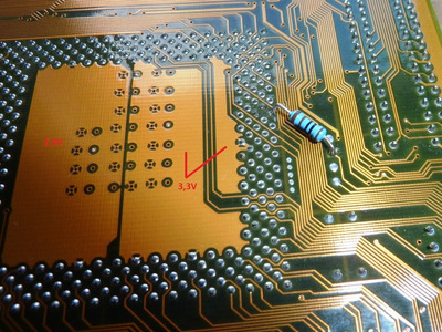
While I was looking for a Vcc3 pin at the CPU for the BF0 mod I found the voltage to be at 3.3V but there´s no direct connection to the 3.3V regulator at the upper-right corner of the board!
So where the hell does the 3.3V I/O-voltage for the CPU come from?

ga5hx_tot.JPG
Filename
ga5hx_tot.JPG
File size
283.33 KiB
Views
1824 views
File license
Fair use/fair dealing exception

I just found the answer myself: If Jumper JP4 is present (and no automatic detection for Split-Voltage CPUs and Core Voltage) JP4 is jumpered so that there´s a double bridge between 3.3V from the regulator and the Vcc3 pins at the CPU socket.
With automatic detection - which is the case here - JP4 is not populated and the 3.3V I/O voltage is switched by the semiconductor In the red circle (probably a MOSFET) by the BIOS autodetection circuit.

ga5hx_vcc3.JPG
Filename
ga5hx_vcc3.JPG
File size
224.67 KiB
Views
1811 views
File license
Fair use/fair dealing exception

Reply 1 of 71, by snufkin

User metadata
Rank Oldbie
Rank
Oldbie

Nice. I came across something similar on the RAM supply on a Slot A board when I was trying to trace that. There was a dual n/p FET that meant the system could swap the supply for the SDRAM between a 3.3V that powered the whole board, or a 3.3V supply generated from the 5VSB. I assume that was to allow sleep mode to work correctly. Oddly, that 9936 is apparently a dual n-type FET, so to switch between supplies it'll need two separate inputs, when an n/p type needs just one input wired to both gates (gate high selects the n side, gate low selects the p side). Maybe that 7404 NOT gate nearby gets involved since they'd need to make sure it wasn't possible to accidentally select both supplies at the same time. I guess that the BIOS won't get involved with the voltage selection, but it'd be handled by the Vcc2Det and VccH/L# pins on the CPU.

Reply 2 of 71, by Sphere478

User metadata
Rank l33t++
Rank
l33t++

interesting

so that board is unable to set 1.5/3.5x or something? (trying to understand the need for resistor mod)

so bf0, bf1, bf2 are three position registers? pull up, open, pull down?

Sphere's PCB projects.
-
Sphere’s socket 5/7 cpu collection.
-
SUCCESSFUL K6-2+ to K6-3+ Full Cache Enable Mod
-
Tyan S1564S to S1564D single to dual processor conversion (also s1563 and s1562)

Reply 3 of 71, by majestyk

User metadata
Rank Oldbie
Rank
Oldbie

There are no options für the voltages in the BIOS menu (like ABIT BIOSes have), there´s only a message at startup like "Voltage Auto-Detect".
On mainboards with BIOS involved there´s typically more circuitry like PALs involved. On the GA-586HX it´s all quite simple and just replaces the Jumpers JP4, so I think you are 100% correct here.

BF2 is not supported by this mainboard, hence there are only 1.5x, 2x, 2,5x and 3x multipliers available using BF0 and BF1 (2² different settings with 2 jumpers and 2 positions: closed or open=floating) .
Earlier CPUs knew the BF-states "Jumper closed" and "jumper floating". That´s why mainboard vendors didn´t care about the trure state of the BF-pins in the jumper open position. This changed with the Pentium MMX that distinguishes between "Jumper closed = BF-pin grounded" and "jumper open = BF pin pulled up to Vcc.
Since the pull up isn´t provided by the mainboard here, multiplier 1.5 x = 3.5x (BF0 open) is not applied by the CPU unless the pullup resistor is added.

Last edited by majestyk on 2022-01-08, 15:15. Edited 2 times in total.

Reply 4 of 71, by Sphere478

User metadata
Rank l33t++
Rank
l33t++
majestyk wrote on 2022-01-08, 15:04:
There are no options für the voltages in the BIOS menu (like ABIT BIOSes have), there´s only a message at startup like "Voltage […]
Show full quote

There are no options für the voltages in the BIOS menu (like ABIT BIOSes have), there´s only a message at startup like "Voltage Auto-Detect".
On mainboards with BIOS involved there´s typically more circuitry like PALs involved. On the GA-586HX it´s all quite simple and just replaces the Jumpers JP4, so I think you are 100% correct here.

BF2 is not supported by this mainboard, hence there are only 1.5x, 2x, 2,5x and 3x multipliers using BF0 and BF1 (2² different settings with 2 jumpers and 2 positions: closed or open=floating) .
Earlier CPUs knew the BF-states "Jumper closed" and "jumper floating". That´s why mainboard vendors didn´t care about the trure state of the BF-pins in the jumper open position. This changed with the Pentium MMX that distinguishes between "Jumper closed = BF-pin grounded" and "jumper open = BF pin pulled up to Vcc.
Since the pull up isn´t provided by the mainboard here, multiplier 1.5 x = 3.5x is not applied by the CPU unless the pullup resistor is added.

Thanks 😀

Sphere's PCB projects.
-
Sphere’s socket 5/7 cpu collection.
-
SUCCESSFUL K6-2+ to K6-3+ Full Cache Enable Mod
-
Tyan S1564S to S1564D single to dual processor conversion (also s1563 and s1562)

Reply 5 of 71, by majestyk

User metadata
Rank Oldbie
Rank
Oldbie

After the MMX233 was up and running it was time for the Tillamook 266.
There are just two tweaks necessary to get it running on this board:

1. To adjust the core-voltage to 1.8V a 100R resistor must be placed in parallel with R127. I soldered a small 2-pin connector in this place so resistors can be adapted to different CPUs / core-voltages.

2. Multiplier x4 has to be enabled by bridging CPU Pin "BF2" with Vss.
Once BF2 is active the Tillamook won´t respond to ANY changes at BF0 and BF1.

ga586hx_r.JPG
Filename
ga586hx_r.JPG
File size
202.46 KiB
Views
1713 views
File license
Fair use/fair dealing exception

The voltage regulator now has to dissipate the heat of a higher voltage drop, 5V - 1.8V = 3.2V instaed of 5V - 2,8V = 2.2V when a regular MMX is present.
But there´still less heat generated in total since the Tillamook´s core draws far less current.

ga586hx_a.JPG
Filename
ga586hx_a.JPG
File size
120.77 KiB
Views
1713 views
File license
Fair use/fair dealing exception
ga586hx_b.JPG
Filename
ga586hx_b.JPG
File size
153.55 KiB
Views
1713 views
File license
Fair use/fair dealing exception
ga586hx_c.JPG
Filename
ga586hx_c.JPG
File size
159.57 KiB
Views
1713 views
File license
Fair use/fair dealing exception

It´s a pity you´re stuck at 66MHz FSB here (unless the clock-generator chip is replaced) plus you´re limited to x4 as maximum multiplier.

Here´s a patched BIOS that supports harddrives up to 137GB and AMD K6-2+ and 3+ CPUs.

http://www.ryston.cz/petr/bios/

I will try this BIOS next, maybe a K6-3+ can run @ 6x66 = 400MHz then?

Last edited by majestyk on 2022-01-09, 19:16. Edited 1 time in total.

Reply 6 of 71, by majestyk

User metadata
Rank Oldbie
Rank
Oldbie

I tested this BIOS, AMD K6-2+ and -3+ are being identified correctly, they can even be configured to run at 400 MHz.
I just tried with a K6-III+ 450 (1.7V core that is quite happy with my current 1.8V setting):

ga586hx_6plus1.JPG
Filename
ga586hx_6plus1.JPG
File size
114.62 KiB
Views
1682 views
File license
Fair use/fair dealing exception
ga586hx_6plus2.JPG
Filename
ga586hx_6plus2.JPG
File size
148.54 KiB
Views
1682 views
File license
Fair use/fair dealing exception

Now that´s a great score!
I don´t think you can push the trusty old Gigabyte GA-586HX (1.53) much further without modding the clock generator for 75 MHz FSB.

The core voltage regulator is stressed much more with a K6-III+ compared to the Tillamook.
A much bigger heatsink or - better - a step-down (buck) regulator would be the perfect solution.

Reply 7 of 71, by Sphere478

User metadata
Rank l33t++
Rank
l33t++
majestyk wrote on 2022-01-09, 16:21:
I tested this BIOS, AMD K6-2+ and -3+ are being identified correctly, they can even be configured to run at 400 MHz. I just trie […]
Show full quote

I tested this BIOS, AMD K6-2+ and -3+ are being identified correctly, they can even be configured to run at 400 MHz.
I just tried with a K6-III+ 450 (1.7V core that is quite happy with my current 1.8V setting):

ga586hx_6plus1.JPG

ga586hx_6plus2.JPG

Now that´s a great score!
I don´t think you can push the trusty old Gigabyte GA-586HX (1.53) much further without modding the clock generator for 75 MHz FSB.

The core voltage regulator is stressed much more with a K6-III+ compared to the Tillamook.
A much bigger heatsink or - better - a step-down (buck) regulator would be the perfect solution.

Yep that’s about all you are going to get out of that board. Look up the clock gen maybe there is a undocumented setting for it that can be achieved by pulling a pin to ground. I discovered a undocumented setting by shorting a pin on my iwill p55xb2 but it wasn’t any use just a weird 320mhz option I think it was. Proof of concept though.

Thank goodness for the k63+ cpus.too bad that they never gave them higher multiplier options.

Sphere's PCB projects.
-
Sphere’s socket 5/7 cpu collection.
-
SUCCESSFUL K6-2+ to K6-3+ Full Cache Enable Mod
-
Tyan S1564S to S1564D single to dual processor conversion (also s1563 and s1562)

Reply 8 of 71, by majestyk

User metadata
Rank Oldbie
Rank
Oldbie

Here´s an old archived site (German only) where they found pin-compatible clock-gens with 75 / 83 MHz.
This would speed up the whole system and allow the K6-III+ to run at 500 MHz!

http://web.archive.org/web/20070808045424/htt … n/busclock.html

And this is why everybody back in the days prefered the ASUS P/I-P55T2P4 for upgrades - it already features 75 MHz and 83 MHz.
The build quality, layout and features of the Gigabyte GA-586HX are excellent otherwise.
These were still "Made In Taiwan" and you can see and feel the very high quality.

I don´t think i´ll mod the clock-generator of this GA-586HX, but I`m going to add USB-support.

Reply 9 of 71, by Sphere478

User metadata
Rank l33t++
Rank
l33t++
majestyk wrote on 2022-01-09, 18:54:
Here´s an old archived site (German only) where they found pin-compatible clock-gens with 75 / 83 MHz. This would speed up the w […]
Show full quote

Here´s an old archived site (German only) where they found pin-compatible clock-gens with 75 / 83 MHz.
This would speed up the whole system and allow the K6-III+ to run at 500 MHz!

http://web.archive.org/web/20070808045424/htt … n/busclock.html

And this is why everybody back in the days prefered the ASUS P/I-P55T2P4 for upgrades - it already features 75 MHz and 83 MHz.
The build quality, layout and features of the Gigabyte GA-586HX are excellent otherwise.
These were still "Made In Taiwan" and you can see and feel the very high quality.

I don´t think i´ll mod the clock-generator of this GA-586HX, but I`m going to add USB-support.

Sweet!! You should do it!!!

I’m still hopping to find a compatible clock gen for my tyan s1564d
Re: New clock gen for tyan s1564d

Sphere's PCB projects.
-
Sphere’s socket 5/7 cpu collection.
-
SUCCESSFUL K6-2+ to K6-3+ Full Cache Enable Mod
-
Tyan S1564S to S1564D single to dual processor conversion (also s1563 and s1562)

Reply 10 of 71, by snufkin

User metadata
Rank Oldbie
Rank
Oldbie
Sphere478 wrote on 2022-01-09, 19:19:

I’m still hopping to find a compatible clock gen for my tyan s1564d
Re: New clock gen for tyan s1564d

Reading that GA-586 mod page it sounds like it has a similar chip, except it uses the 48MHz output when your board needs a 12MHz output for the keyboard.

Go on, see if you can find one of those PLL52C59-14A chips (that's the one I found last, and is mentioned on that GA-586 page, and it looks like it does need to be the 14A version to get 83MHz), then lift the 48MHz output pin and sort out generating the 12MHz keyboard clock. Pretty sure you'd just need either a dual flip-flip and a bit of wiring to divide the 48MHz clock by 4 (e.g. https://uk.farnell.com/texas-instruments/sn74 … 1621017?st=7474 ) or if the keyboard doesn't need to be in phase with the main clock (seems likely) then just a 12MHz oscillator (e.g. https://uk.farnell.com/ael-crystals/o12m00000 … 2mhz/dp/9510117 ).

I ran that modding page through Google translate for the later mod where they swap out the 14.318MHz crystal for a 20MHz version, because I was pretty sure I was reading it wrong. Swapping the crystal overclocks the bus, but also stops the floppy and serial ports working, so they wanted to reintroduce the 14MHz signal. So, if Google translate has this right, they take a broken motherboard and use a saw to cut out the bit of the PCB holding the clock generator and crystal, then use that PCB fragment and wire it up to the modded board. Exciting. Wish there were photos.

Reply 11 of 71, by majestyk

User metadata
Rank Oldbie
Rank
Oldbie

Problem is these clock generator chips are extremely hard to find today.

clock_chips.JPG
Filename
clock_chips.JPG
File size
22.22 KiB
Views
1572 views
File license
Public domain

And I would never slaughter a FIC PA-2005, ABIT PR5 or ASUS P55T2P4 rev.3.0 just to harvest the clock-generator for a GA-586HX. That would be quite pointless and I´de rather repair the donor board.
And there´s one more risk: We can´t be sure the GA-586HX will be running stable at 75 or even 83 MHz. The layout must support higher frequencies, the chipset, SRAM and TAG-RAM chips etc.
And the whole effort would be justified only if 83 MHz would be a stable option, the difference between 66 and 75 MHz is too slim to bother.

Gigabyte decided not to support FSBs >66MHZ even on their GA-586HX 2.01 revision that was redesigned in many aspects.

Reply 12 of 71, by snufkin

User metadata
Rank Oldbie
Rank
Oldbie

Agree about not harvesting parts, unless the board's too far gone (like snapped in half or something). Probably don't need to though, just vary the second method on that page of replacing the main crystal with the clock gen from another board that provides the non-CPU&Bus clocks and also provides a 20MHz input to the existing clock gen.

If I understand rightly, the standard clock gen can do CPU clock of 50, 55, 60 and 66.7MHz with the bus at half that? But it also provides a couple of 14.318MHz reference outputs, a 48MHz USB and 24MHz chipset clock. That mod page doesn't mention the 48MHz USB clock, and the Intel datasheet gives a register that can be set to select either 24 or 48MHz as the USB clock source. Which means possibly just the 24 and 14.318MHz need to be provided (could tell better if it's possible to see if any tracks are routed out from the 48MHz output).

So just lift the output pins on the clock gen and get two oscillators at 14.318MHz and 24MHz and connect them to appropriate PCB pads. Then replace the existing 14.318 crystal with a 20MHz crystal (maybe put it in a socket). That would give CPU clock options from around 70 to 93MHz, which if the board's stable at 66.7 should give at least one stable point at 70MHz. And it wouldn't make any permanent changes to the board either.

Reply 14 of 71, by snufkin

User metadata
Rank Oldbie
Rank
Oldbie

Certainly PCI. A skim of the 82371 datasheet says that ISA is either PCI/3 or PCI/4, so it sounds like that would over clock as well. That mod site mentions about on Intel chipsets the PCI bus needs to be synchronous with the CPU clock, so it's fixed by the clock gen at 1/2 CPU. The -14A version has a couple of asynchronous options that keep the bus clock at 33MHz, but they probably won't work with the chipset.

That German site claimed their board was stable at a CPU clock of 93.3, which would have had the PCI bus at 46.7MHz. It affects so many things (IDE interface as well I think) that it'll be pot luck how fast the bus can go, and figuring out what the limit is would be a pain. OTOH, Anandtech page about the 430HX says that it was the first chipset to unofficially support 83.3MHz CPU clock speeds: https://www.anandtech.com/show/72/5

Reply 15 of 71, by majestyk

User metadata
Rank Oldbie
Rank
Oldbie

Maybe it´s a better idea to try a clock-gen mod with a GA-586HX Rev. 2.01.

It has a stepdown voltage regulator for voltages down to 2.0V already onboard so K6-2+ and K6-III+ CPUs can be used out of the box (without the need of enhanced cooling for the linear regulator).

ga_586hx_201vrm.JPG
Filename
ga_586hx_201vrm.JPG
File size
440.26 KiB
Views
1490 views
File license
Fair use/fair dealing exception
ga_586hx_201vsw.JPG
Filename
ga_586hx_201vsw.JPG
File size
231.76 KiB
Views
1490 views
File license
Fair use/fair dealing exception

In the Intersil datasheet for the HIP6008 you can find a nice ready designed application:

vrm_hp6008.JPG
Filename
vrm_hp6008.JPG
File size
86.79 KiB
Views
1474 views
File license
Public domain

The clock generator section seems to be the same - it uses the same Phaselink circuit but without tho option to use manual jumpers insted of the double switch and without options for 50 MHz and 55 MHz:

ga_586hx_201clock.JPG
Filename
ga_586hx_201clock.JPG
File size
505.05 KiB
Views
1490 views
File license
Fair use/fair dealing exception

Without modifying it you´re restricted to 66,6 x 6 = 400 MHz which is a pity. At 83,3 MHz FSB the CPUs could operate at 500 MHz.

Reply 16 of 71, by snufkin

User metadata
Rank Oldbie
Rank
Oldbie

I just realised that I can't find a datasheet for the -14L, so don't actually know if pin 5 is an Output Enable signal (like on e.g. ICS9159C-02) or a Turbo/FSEL2 pin like on the other PLL52C59-14 chips. Do you know if pin 5 is floating or pulled to Vdd? I can't see any surface traces going to it, but there may be one underneath the chip connecting it directly to Vdd (maybe short to pin 1 or 8, or to +5).

To switch between 60 and 66 then I think inputs to R151 and R152 must be inverted and controlled by SW1 (so they switch from 01 to 10), and looking at another photo it looks like there's a FET (Q9? photo I'm looking at is a bit blurry) near SW1 that probably does the inverting.

If you did manage to get your hands on either a PLL52C59-14A or ICS9159C-14 then you'd need to figure out a mod around SW1 to stop it inverting the FSEL[1..0] signals, since you'd want them to be 00 or 11. You'd also need a safe way to pull pin 5 (FSEL2) low. That'll be easy if the board currently relies on an internal pull up as you can just ground the pin, but slightly more complicated if it's tied directly to Vdd as you'd need to lift the pin and make sure it can't ever short back to the pad.

If you went the changing the crystal route, then it looks like only one of the two reference clock outputs is used, and the 24MHz output. So that'd mean lift pin 28 and 24, then inject a 14.318 signal to R61/R62 and a 24MHz signal to R34. You'd need to check if the other reference output (pin 27) or the 48MHz output (pin 25) are actually used and the tracks are under the chip. Incidentally, is there something odd about the soldering between pin 20 and 21?

I'm confused by the board markings for the voltage, it looks like 2.8V and Auto have the same settings.

Reply 17 of 71, by majestyk

User metadata
Rank Oldbie
Rank
Oldbie

At Pin 5 I measure 0.65V so I guess it´s floating.
Transistor Q9 is "1AM x" (x is hard to decipher, looks like a tiny "6"), but it´s probably just 1AM, a regular NPN transistor.
With S1 in position "off" (66 MHz) there´s 0V at all pins, with S1 in position "on" (60 MHz) there´s 0V at B and E and 0.4V at C.

Thanks for the hint that the "S1 circuit" for FSEL0 and FSEL1 would also need a modification!

I just carefully cleaned the space between Pin 20 and 21 with 99% Isoprop. and a small brush and removed whataever it was.

Last edited by majestyk on 2022-01-14, 15:33. Edited 1 time in total.

Reply 18 of 71, by snufkin

User metadata
Rank Oldbie
Rank
Oldbie
majestyk wrote on 2022-01-14, 14:28:
At Pin 5 I measure 0.65V so I guess it´s floating. Transistor Q9 is "1AM x" (x is hard to decipher, looks like a tiny "6"), but […]
Show full quote

At Pin 5 I measure 0.65V so I guess it´s floating.
Transistor Q9 is "1AM x" (x is hard to decipher, looks like a tiny "6"), but it´s probably just 1AM, a regular NPN transistor.
With S1 in position "off" (66 MHz) there´s 0V at all pins, with S1 in position "on" (60 MHz) there´s 0V at B and E and 0.4V at C.

Thanks for the hint that the "S1 circuit" for FSEL0 and FSEL1 would also need a modification!

I just carefully cleaned the space between Pin 20 and 21 with 99% Isoprop. and a small brush and removed whataever it was.

So you can probably connect pin 5 to ground, perhaps through a 10k resistor (internal pull up will probably be weaker than that) and see what happens. There's a good chance that it's actually an OE pin and so nothing will work because all the clocks are off, but if you do try it then measure the voltage on pin 5, and try with SW1 in both positions.
Any chance of a photo of the area around SW1? It sounds like I'm wrong about that transistor being use to invert FSEL0 from FSEL1. Probably also worth checking the voltages at FSEL0 and 1 (pins 13 and 12) to see if I'm at least right that one will be '1' and the other '0'.

Reply 19 of 71, by majestyk

User metadata
Rank Oldbie
Rank
Oldbie

O.k. FET-VOM has got a new battery now and I can correct the voltages at FSEL0 and FSEL1:

At 60 MHz (S1 on) there´s 0V at pin 13 and 1.7V at pin 12
At 66 MHz (S1 off) it´s 2.1V at pin 13 and 0.1V at pin 12.

So the two signals a r e inverted. There´s also 0 Ohms between Collector of Q9 and pin 12 of the clock-gen chip - your theory of Q9 inverting the signal is alive again.

I must also correct the voltages at Q9:

60 MHz:
C = 1.7V
E = 0V
B = 0V

66 MHz:
C = 0.1V
E = 0V
B = 0.6V

ga_586hx_201sw.JPG
Filename
ga_586hx_201sw.JPG
File size
742 KiB
Views
1404 views
File license
Fair use/fair dealing exception