VOGONS


286 motherboard repairs

Topic actions

First post, by Skip94

User metadata
Rank Newbie
Rank
Newbie

Hi all
A friend has asked me if I can repair a 286 motherboard that was in an IBM 5170 case he bought. I've done a bit of work so far, but no success.
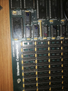
The board is branded "Western computer 286 turbo". I can find zero information about it online.
So far I have;
Given the board a thorough wash, as it was filthy.
Cleaned all the socket contacts with phosphoric acid gel, as a lot were mildly corroded. They all now look fine. I also sanded all the legs of the chips before refitting to clean them up.
All 74 series logic chips have been tested as good in my TL866.
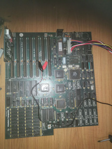
The CPU has been swapped for a known good one
The BIOS has been read and it looks to be ok. Having had a lot of luck swapping 286 BIOS's in the past, I have tried a few different BIOS images for the same chipset in there.
I have tried to use the Landmark diagnosic ROMs, but with them installed, there is no activity on a POST card.

So, the symptoms...
It powers on and all voltages seem good. The post card displays codes for a brief moment before freezing on 02. For the first few seconds, there is activity on the address and data bus pins on the CPU, then it just goes high, a couple seconds after the 02 code appears on the POST card.
The CPU is recieving a clock signal according to my logic probe. There is no display on the screen and as far as I can tell, no PC speaker beep, although the PC speaker header isn't labelled, so I've just tried all 4 pin headers I can see.
There is no obvious damage to the board, luckily it has never had a battery installed
I have also removed all the RAM to test, but this hasn't affected anything, it seems to not even be getting that far.
I'm a little stumped where to go next. I assume one of the less generic chips has failed, but I'd rather diagnose further, rather than just start replacing bits, hoping for the best.
Any thoughts?
Cheers
Andrew

Attachments

Reply 1 of 66, by Predator99

User metadata
Rank l33t
Rank
l33t

Landmark is a good point to start. There will be no output on the POST-card with it. You get a display only on MDA/CGA or you hear output from the speaker. You need to be patient, it may take some time until it starts.

Reply 2 of 66, by Deunan

User metadata
Rank Oldbie
Rank
Oldbie

These old PCBs can have subtle damage like cracked traces or vias that are rather difficult to find. It's possible, and a good project for someone who has the patience to go slow and can switch to other things when it's not going well. Otherwise it can be pretty frustrating.

What I do with such cases is write a small program in assembly and put it in place of BIOS ROMs (at 0xFFFF0 obviously) - you can easily have some output via the POST card by doing OUT to port 0x80 with a value you've chosen. If that works, then the ROM is being read properly, or at least this part of it. Then you can check if all of it works by doing some pattern or checksum. After that it should be possible to do some rudimentary RAM check, but since you didn't start the refresh HW yet you can only do R/W pattern tests on one location and move on. With this working you should be getting some output with diagnostic ROMs or even the original BIOS.

Things to keep in mind: ROMs on 286 mobos are usually split into even/odd bytes to allow full 16-bit access from CPU for speed. This means any code you want to try must be properly split into two images (as in, bytes 0,2,4... etc go into EVEN and 1,3,5... into ODD). Also, the EVEN/ODD stickers or mobo markings might be misleading, so do try swapping the chips around if nothing works.

If assembly is not your thing, here's a simple code and the binary output: mov al,0x34 | out 0x80,al | mov al,0x12 | out 0x80,al | hlt -> B0 34 E6 80 B0 12 E6 80 F4
Try pasting that over the original BIOS image in the hex editor, at 8 bytes from the end of the images. So on EVEN image at -8 from end you should be seeing EA, overwrite with B0 E6 B0 E6 F4, and on the ODD one at the same location put 34 80 12 80. See if that outputs 1234 to POST card display.

EDIT: Or you can upload your EVEN/ODD ROMs here, I can both test the checksum and mod them for you if you wish.

Reply 3 of 66, by snufkin

User metadata
Rank Oldbie
Rank
Oldbie

That low level testing sounds good.

Could also be a CMOS problem maybe (looks like some Pheonix BIOS use 02 as a CMOS read/write test)? Maybe it needs a battery on the external header (if it has one, J21?) or the BATT1 position? Looks like the CMOS/RTC chip is between the keyboard connector and the battery, might be one of these: https://www.nxp.com/docs/en/data-sheet/MC146818.pdf . Or one of the RAM chips went bad?

If there's an 82A203 chip on the board then pin 59 is SPKRDATA. If that goes to a header then you'll know where the speaker goes.

Reply 4 of 66, by computerguy08

User metadata
Rank Member
Rank
Member
Deunan wrote on 2022-01-27, 09:48:
These old PCBs can have subtle damage like cracked traces or vias that are rather difficult to find. It's possible, and a good p […]
Show full quote

These old PCBs can have subtle damage like cracked traces or vias that are rather difficult to find. It's possible, and a good project for someone who has the patience to go slow and can switch to other things when it's not going well. Otherwise it can be pretty frustrating.

What I do with such cases is write a small program in assembly and put it in place of BIOS ROMs (at 0xFFFF0 obviously) - you can easily have some output via the POST card by doing OUT to port 0x80 with a value you've chosen. If that works, then the ROM is being read properly, or at least this part of it. Then you can check if all of it works by doing some pattern or checksum. After that it should be possible to do some rudimentary RAM check, but since you didn't start the refresh HW yet you can only do R/W pattern tests on one location and move on. With this working you should be getting some output with diagnostic ROMs or even the original BIOS.

Things to keep in mind: ROMs on 286 mobos are usually split into even/odd bytes to allow full 16-bit access from CPU for speed. This means any code you want to try must be properly split into two images (as in, bytes 0,2,4... etc go into EVEN and 1,3,5... into ODD). Also, the EVEN/ODD stickers or mobo markings might be misleading, so do try swapping the chips around if nothing works.

If assembly is not your thing, here's a simple code and the binary output: mov al,0x34 | out 0x80,al | mov al,0x12 | out 0x80,al | hlt -> B0 34 E6 80 B0 12 E6 80 F4
Try pasting that over the original BIOS image in the hex editor, at 8 bytes from the end of the images. So on EVEN image at -8 from end you should be seeing EA, overwrite with B0 E6 B0 E6 F4, and on the ODD one at the same location put 34 80 12 80. See if that outputs 1234 to POST card display.

EDIT: Or you can upload your EVEN/ODD ROMs here, I can both test the checksum and mod them for you if you wish.

I've been fighting a similar level of issues with some 386 boards and I tried the trick you mentioned here with the assembly code, but on mine it doesn't even do that.

Reply 5 of 66, by Deunan

User metadata
Rank Oldbie
Rank
Oldbie

Well, with a 386 mobo (unless it's a very early adaptation of 286 chipset) you probably have only one BIOS ROM? In that case you need to put the code at -16 bytes from the end. And if that doesn't work I would suggest making sure all the ROM chip/socket pins are connected somewhere to the chipset. And/or, if you have a scope, checking if the control and address lines toggle (at all, and then correctly or not but that is harder to properly setup).

Reply 6 of 66, by Skip94

User metadata
Rank Newbie
Rank
Newbie
Predator99 wrote on 2022-01-27, 08:06:

Landmark is a good point to start. There will be no output on the POST-card with it. You get a display only on MDA/CGA or you hear output from the speaker. You need to be patient, it may take some time until it starts.

Thank you. I was trying with a Hercules card, but I wonder if that isn't compatible. I have a genuine IBM MDA card and 5151 monitor here, so I'll borrow them from my 5160 and try that first. Interesting that it doesn't give an output on the POST card, I kind if assumed no output = no life.
I shall let that run for a few minutes when I get a chance.
Cheers
Andrew

Reply 7 of 66, by Skip94

User metadata
Rank Newbie
Rank
Newbie
Deunan wrote on 2022-01-27, 09:48:
These old PCBs can have subtle damage like cracked traces or vias that are rather difficult to find. It's possible, and a good p […]
Show full quote

These old PCBs can have subtle damage like cracked traces or vias that are rather difficult to find. It's possible, and a good project for someone who has the patience to go slow and can switch to other things when it's not going well. Otherwise it can be pretty frustrating.

What I do with such cases is write a small program in assembly and put it in place of BIOS ROMs (at 0xFFFF0 obviously) - you can easily have some output via the POST card by doing OUT to port 0x80 with a value you've chosen. If that works, then the ROM is being read properly, or at least this part of it. Then you can check if all of it works by doing some pattern or checksum. After that it should be possible to do some rudimentary RAM check, but since you didn't start the refresh HW yet you can only do R/W pattern tests on one location and move on. With this working you should be getting some output with diagnostic ROMs or even the original BIOS.

Things to keep in mind: ROMs on 286 mobos are usually split into even/odd bytes to allow full 16-bit access from CPU for speed. This means any code you want to try must be properly split into two images (as in, bytes 0,2,4... etc go into EVEN and 1,3,5... into ODD). Also, the EVEN/ODD stickers or mobo markings might be misleading, so do try swapping the chips around if nothing works.

If assembly is not your thing, here's a simple code and the binary output: mov al,0x34 | out 0x80,al | mov al,0x12 | out 0x80,al | hlt -> B0 34 E6 80 B0 12 E6 80 F4
Try pasting that over the original BIOS image in the hex editor, at 8 bytes from the end of the images. So on EVEN image at -8 from end you should be seeing EA, overwrite with B0 E6 B0 E6 F4, and on the ODD one at the same location put 34 80 12 80. See if that outputs 1234 to POST card display.

EDIT: Or you can upload your EVEN/ODD ROMs here, I can both test the checksum and mod them for you if you wish.

Thanks
I'm quite happy to plod away with this, I'd really like to get it working. I shall bring it into work one day and have a look under the magnifier at all the pads/vias etc.
I had heard of modding the ROMs to do that, but I'll admit it was a little over my head. Thanks to your explanation, I'm going to have a go at that and if I get nowhere, I'll upload them for you to have a look at.
Showing my lack of knowledge, why at the end, is that where the code starts from?
Thanks
Andrew

Reply 8 of 66, by Skip94

User metadata
Rank Newbie
Rank
Newbie
snufkin wrote on 2022-01-27, 10:23:

That low level testing sounds good.

Could also be a CMOS problem maybe (looks like some Pheonix BIOS use 02 as a CMOS read/write test)? Maybe it needs a battery on the external header (if it has one, J21?) or the BATT1 position? Looks like the CMOS/RTC chip is between the keyboard connector and the battery, might be one of these: https://www.nxp.com/docs/en/data-sheet/MC146818.pdf . Or one of the RAM chips went bad?

If there's an 82A203 chip on the board then pin 59 is SPKRDATA. If that goes to a header then you'll know where the speaker goes.

Thanks.
It is indeed a Phoenix BIOS, I'd seen that 02 means CMOS RAM issues. I assume that means the few bytes of RAM in the CMOS chip itself, as the test of the 1st 4k of normal RAM is further down the POST order. Having conventional RAM installed seems to make absolutely no difference.
I have tried a battery on it, although only a 3v coin cell. It also seemed to make no difference. There is no evidence of a battery ever having been installed on the board, so I just soldered pin headers onto the battery silkscreen markings.
I shall trace that line out of the 203 chip to find the speaker, thanks for that!
Cheers
Andrew

Reply 9 of 66, by Deunan

User metadata
Rank Oldbie
Rank
Oldbie
Skip94 wrote on 2022-01-27, 23:50:

Showing my lack of knowledge, why at the end, is that where the code starts from?

A quirk of x86 family of CPUs, they have the reset vector at the end of their address space -16 bytes rather than zero. My guess is it was done to make it easier to implement CP/M (or DOS) that need to have RAM at low addresses, and CPUs like Z80 had to resort to memory banking and copying ROM ro RAM to overcome that. This scheme also lets you keep the ROM in that place rather than swapping it out for RAM (since x86 had "plenty" of address space and was not limited to 64KiB, even if each segment can only be that big). Although that's exactly what more modern 386+ systems do, it's called ROM shadowing and makes the access faster since RAM uses full width of data bus and ROMs are only 8-bit on these newer machines. BTW another quirk of x86 is it will actually lock all the address lines except the few lowest ones at 1 after reset and only a far jump can unlock that. So all PC BIOSes have a far jump as the very first instruction.

Note, I said at the end of address space, not end of the first megabyte, so on 286 that would make the reset vector be 16MiB - 16 bytes, but you don't need to worry about that. Motherboard chipset will re-map that to the end of first megabyte, so it works just like on 8086. Therefore from software point of view the reset vector is still 0xFFFF0 in linear addressing.

One more thing, when you replace the original BIOS ROMs/EPROMs with something else, do make sure you've picked the correct size chips. Those ROMs are usually 32KiB each but some earlier 286 BIOSes were smaller and used 16KiB chips (for total of 32KiB image). There's usually jumpers on the mobo to select correct chip size, but even without those it's possible to use chips with more capacity so long you remember to mirror/repeat the image in them. And also make sure to use the "EPROM emulator" chips rather than modern FLASH or EEPROM parts directly, as these have sligtly different pinout. This might be obvious to you but I figured I'd mention it before suggesting more involved testing methods.

Reply 10 of 66, by Skip94

User metadata
Rank Newbie
Rank
Newbie

Thanks, thats interesting. I haven't had a chance to do that yet, but will over the weekend.
The chips removed were 27C256's, so 32k. I have replaced them with 28C256 EEPROMS for convenience, fitted in an adaptor to change the pinout to 27C256. I've tested these on my other 286 board that originally used 27C256 EPROMS and they work fine. Writing the original BIOS code read from the EPROMS onto these 28C256's in the adaptors results in exactly have same sequence of events as with the originals fitted.
I did get a few minutes on it this morning, and have done the following.
tried to follow where pin 59 on the P82A203 goes to find the speaker output. No joy, its not connected directly to any of the pin headers on the board. I haven't yet been able to follow the trace, as it is hidden under the socket.
I flashed the Landmark diagnostics onto the EEPROMS again and left it running with an IBM MDA adaptor and 5151 monitor for several minutes. Nothing. Activity on the address lines stops after a few seconds and stays like that.
I have swapped out the HD146818P CMOS/RAM chip. A quick bit of googling suggests that it is compatible with the Dallas 1287. So I robbed one out of my 486 and stuck that in. No change.
Andrew

Reply 11 of 66, by snufkin

User metadata
Rank Oldbie
Rank
Oldbie

I'm sure you know already, but mind that pin 1 of the 203 starts in the middle of one side. It's a minor thing really as hopefully you'll be able to get more information out via the POST card soon, but if you post some photos of the front and back around the 203 might help tracing the speaker signal.

Reply 12 of 66, by Skip94

User metadata
Rank Newbie
Rank
Newbie
Deunan wrote on 2022-01-27, 09:48:
These old PCBs can have subtle damage like cracked traces or vias that are rather difficult to find. It's possible, and a good p […]
Show full quote

These old PCBs can have subtle damage like cracked traces or vias that are rather difficult to find. It's possible, and a good project for someone who has the patience to go slow and can switch to other things when it's not going well. Otherwise it can be pretty frustrating.

What I do with such cases is write a small program in assembly and put it in place of BIOS ROMs (at 0xFFFF0 obviously) - you can easily have some output via the POST card by doing OUT to port 0x80 with a value you've chosen. If that works, then the ROM is being read properly, or at least this part of it. Then you can check if all of it works by doing some pattern or checksum. After that it should be possible to do some rudimentary RAM check, but since you didn't start the refresh HW yet you can only do R/W pattern tests on one location and move on. With this working you should be getting some output with diagnostic ROMs or even the original BIOS.

Things to keep in mind: ROMs on 286 mobos are usually split into even/odd bytes to allow full 16-bit access from CPU for speed. This means any code you want to try must be properly split into two images (as in, bytes 0,2,4... etc go into EVEN and 1,3,5... into ODD). Also, the EVEN/ODD stickers or mobo markings might be misleading, so do try swapping the chips around if nothing works.

If assembly is not your thing, here's a simple code and the binary output: mov al,0x34 | out 0x80,al | mov al,0x12 | out 0x80,al | hlt -> B0 34 E6 80 B0 12 E6 80 F4
Try pasting that over the original BIOS image in the hex editor, at 8 bytes from the end of the images. So on EVEN image at -8 from end you should be seeing EA, overwrite with B0 E6 B0 E6 F4, and on the ODD one at the same location put 34 80 12 80. See if that outputs 1234 to POST card display.

EDIT: Or you can upload your EVEN/ODD ROMs here, I can both test the checksum and mod them for you if you wish.

Deunan,
Apologies that its taken so long, the last couple of weeks have been crazy busy.
However, depsite having no idea what I'm doing, your instructions were perfect. Modded the BIOS as you said and now 1234 appears on the post card.
I'm not sure exactly what this is telling me, but I assume that it means the motherboard is working well enough to run that first bit of code and write the correct values to the register that the post card is looking at?
I have uploaded the original two ROM images here anyway, just in case looking through them will help anyone. I've had to save them as .txt files, as it won't allow me to upload bin files here, hope this is ok.
Cheers
Andrew

Attachments

  • Filename
    Original U48.txt
    File size
    32 KiB
    Downloads
    36 downloads
    File license
    Public domain
  • Filename
    Original U47.txt
    File size
    32 KiB
    Downloads
    32 downloads
    File license
    Public domain

Reply 13 of 66, by Skip94

User metadata
Rank Newbie
Rank
Newbie

I have also managed to trace the PC speaker output. Pin 59 on the P82A203, which is SPKRDATA, goes to U63, a NAND gate. The other input for the NAND gate comes from pin 55 on the P82A203, which is labled OUT2.
The output from the NAND gate then goes to an input of a 74LS244 buffer. The output of that runs through a 30 ohm resistor to pin one of a 4 pin header.
Andrew

Reply 14 of 66, by snufkin

User metadata
Rank Oldbie
Rank
Oldbie
Skip94 wrote on 2022-02-06, 05:04:

I have also managed to trace the PC speaker output. Pin 59 on the P82A203, which is SPKRDATA, goes to U63, a NAND gate. The other input for the NAND gate comes from pin 55 on the P82A203, which is labled OUT2.
The output from the NAND gate then goes to an input of a 74LS244 buffer. The output of that runs through a 30 ohm resistor to pin one of a 4 pin header.
Andrew

That's good, you've found the speaker header. I guess OUT2 provides the frequency from a timer in the 203, which is then gated by the on/off signal from SPKRDATA, and the output of the NAND is then buffered so there's enough current to drive the speaker, with a 30ohm resistor to protect against shorts. If the speaker signal goes to pin 1 then you should find that pin 4 goes to +5, and the speaker connects to 1&4.

Hopefully you can get some beeps out of it once the board gets a bit further along the POST.

Reply 15 of 66, by Deunan

User metadata
Rank Oldbie
Rank
Oldbie
Skip94 wrote on 2022-02-06, 04:41:

Modded the BIOS as you said and now 1234 appears on the post card.

Good, that means the CPU is working and fetching instructions, at least it goes this far. I looked at your BIOS image and spotted 2 things right away, it's an early Phoenix BIOS which might not output any codes, I'll check that properly in few hours. Second issue it's actually 32KiB image, should use 2x 16KiB chips. If it uses 2x 32KiB ones then the first half of each chip should be empty (and indeed looks like it's just 0xFF in there). Point is, the mobo is most likely configured for 16KiB ROMs and the A14 line is just held high permanently (because A14 on 27C256 is /PGM on 27C128) - so trying to boot any 64KiB image will not work, and that might be why your diagnostic ROM appears dead.

Solutions for now - if you have that diagnostic ROM as 32KiB image, split it into 2x 16KiB and program into upper halfs of your EPROMs, that should work. If there isn't a smaller version of it, you need to find the manual for mobo jumpers - if there are jumpers, could be the mobo is hardwired for 16KiB chips. Would be somewhat surprising but not impossible. It's also possible to try and figure out which jumper it is by yourself, A14 is pin #27 on the ROMs so see where that goes to. Both chips should share this line BTW.

If you have the time it would also be a good idea to make sure all the A0-A13/A14 lines of the BIOS ROMs are connected somewhere. Since the code I gave you worked it would suggest the lowest address lines (A0-A2) do toggle properly, but the higher-order ones might be stuck (shorted for example) or have broken connections. It would be good to check that.

UPDATE: Something is wrong with these dumps. It's like bit 5 (value 0x20) is stuck high most of the time, but not on all bytes. And on both files too so that's unlikely to be an issue with one of the chips. Poor socket contact in the programmer maybe? Are these the original ROM chips (those usually have stickers) - if you suspect not then perhaps somebody tried a BIOS upgrade but messed up programming the chips, so what you have now is unsuable.

UPDATE 2: I'm starting to wonder if the issue is not with the file extensions and/or forum code. These were attached to the post as TXT files but are obviously not text-only. It looks like all zero bytes were replaces with spaces, which would look very much like bit 5 being stuck high. Some bytes however have values with bit 5 at zero, but those are pretty much all valid text-file control characters like end line, line feed, tab, etc. Could you maybe pack the image into ZIP or 7z archive and attach that instead? But make sure the files are correct on your side - for example U48 last byte should be zero, not 0x20.

Reply 16 of 66, by Skip94

User metadata
Rank Newbie
Rank
Newbie
Deunan wrote on 2022-02-07, 11:15:
Good, that means the CPU is working and fetching instructions, at least it goes this far. I looked at your BIOS image and spotte […]
Show full quote
Skip94 wrote on 2022-02-06, 04:41:

Modded the BIOS as you said and now 1234 appears on the post card.

Good, that means the CPU is working and fetching instructions, at least it goes this far. I looked at your BIOS image and spotted 2 things right away, it's an early Phoenix BIOS which might not output any codes, I'll check that properly in few hours. Second issue it's actually 32KiB image, should use 2x 16KiB chips. If it uses 2x 32KiB ones then the first half of each chip should be empty (and indeed looks like it's just 0xFF in there). Point is, the mobo is most likely configured for 16KiB ROMs and the A14 line is just held high permanently (because A14 on 27C256 is /PGM on 27C128) - so trying to boot any 64KiB image will not work, and that might be why your diagnostic ROM appears dead.

Solutions for now - if you have that diagnostic ROM as 32KiB image, split it into 2x 16KiB and program into upper halfs of your EPROMs, that should work. If there isn't a smaller version of it, you need to find the manual for mobo jumpers - if there are jumpers, could be the mobo is hardwired for 16KiB chips. Would be somewhat surprising but not impossible. It's also possible to try and figure out which jumper it is by yourself, A14 is pin #27 on the ROMs so see where that goes to. Both chips should share this line BTW.

If you have the time it would also be a good idea to make sure all the A0-A13/A14 lines of the BIOS ROMs are connected somewhere. Since the code I gave you worked it would suggest the lowest address lines (A0-A2) do toggle properly, but the higher-order ones might be stuck (shorted for example) or have broken connections. It would be good to check that.

UPDATE: Something is wrong with these dumps. It's like bit 5 (value 0x20) is stuck high most of the time, but not on all bytes. And on both files too so that's unlikely to be an issue with one of the chips. Poor socket contact in the programmer maybe? Are these the original ROM chips (those usually have stickers) - if you suspect not then perhaps somebody tried a BIOS upgrade but messed up programming the chips, so what you have now is unsuable.

UPDATE 2: I'm starting to wonder if the issue is not with the file extensions and/or forum code. These were attached to the post as TXT files but are obviously not text-only. It looks like all zero bytes were replaces with spaces, which would look very much like bit 5 being stuck high. Some bytes however have values with bit 5 at zero, but those are pretty much all valid text-file control characters like end line, line feed, tab, etc. Could you maybe pack the image into ZIP or 7z archive and attach that instead? But make sure the files are correct on your side - for example U48 last byte should be zero, not 0x20.

Thank you!
I have been crazy busy with outdoors projects here, so haven't really had a chance to look at it recently, but we have bad weather due this weekend, so I'll try and have a play. I'll attach the .bin files in a zip when I get home.
I'll also have a play with the diagnostics as you suggest.
Andrew

Reply 17 of 66, by Skip94

User metadata
Rank Newbie
Rank
Newbie

Right...
I have traced pin 27 on both EPROMS to a jumper next to them, with nothing installed. On pin of this is connected to VCC, so I have added a jumper here. There is also a jumper next to it that ties pin 20 Chip enable to ground. I presume this needs adding as well, as CE is active low. I have added this jumper. How much difference has this made? None! I still get a second or so of activity on the address bus, then nowt.
I have looked through the code for the Landmark diagnostics. It is duplicated at address 0000 and at 4000, so should be fine as it is, I think?
I haven't yet checked the address line continuity, I'll do that tonight.
I have attached a zip file of the two original BIOS ROMS
The chips look original.
Andrew

Attachments

Reply 18 of 66, by Deunan

User metadata
Rank Oldbie
Rank
Oldbie
Skip94 wrote on 2022-02-18, 07:21:

I have attached a zip file of the two original BIOS ROMS

The good news: This dump looks good, also the checksum seems correct. The bad: BIOS does write to port 0x80 so should output POST codes. It could be a problem with KBC or the '245 that drives lower 8 bits of ISA bus, but then the Landmark ROM should work - unless it too tries to read the KBC to figure out if the reset was a cold or a warm one and the bit is glitched. Well, your mobo seems socketed so if the programmer you have can test 74xx chips then remove and test the 74ALS245 near KBC and ISA.

As for the jumpers, A14 to Vcc shouldn't be needed for your 32KiB chips but I would expect pin 27 to be connected to something, so if the jumper was completly open before it's weird, possibly someone removed the link. Unless this pin has a pull-up resistor independent of the jumper position. And yes, if Landmark is copied twice in the image (at 0x0000 and 0x4000) then it too should work.

I'm not sure what the jumper for /CE line (pin 20) is for. Sometimes that pin is connected to GND directly at the chip, true, but maybe leave it as it was for now, possibly the chipset is driving it - I mean my code did work without it, right? But keep it in mind. If you have some time for more testing during the weekend, and some chips you can program, I can write a more advanced test "BIOS" for you. Nothing like the Landmark, just some more POST codes.

Reply 19 of 66, by Skip94

User metadata
Rank Newbie
Rank
Newbie

Deunan, I shall pull that 74ALS245 and test it again, although I have been through and checked all 74 series chips before.
Do I recall that keyboard controllers are for the most part interchangeable? Would it be worth trying a different one?
I'd really appreciate a more advanced test BIOS. I'm currently using 28C256's in adaptors, so reprogramming them is very simple.
Cheers
Andrew