Reply 40 of 221, by Kahenraz

Rank
l33t
- Rank
- l33t
I bought a couple of these from a recycler some time ago, so I'm happy to experiment on one of them.
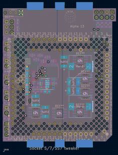
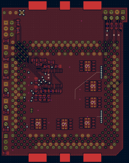
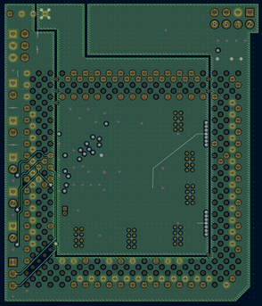
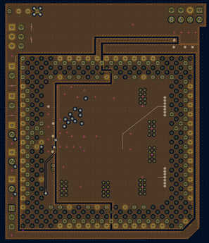
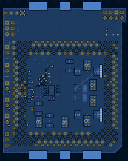
I really like these boards so it's exciting to think about making improvements to it and seeing how far it'll go. It's an Intel OEM board, the quality of which is excellent, and there is also a hidden surprise. It has 3.3v on the PCI slots! For an early Socket 7 motherboard, there is so much potential.