VOGONS


Fixing up a Soyo SY-5TF Socket 7 Motherboard

Topic actions

Reply 20 of 240, by Sphere478

User metadata
Rank l33t++
Rank
l33t++
majestyk wrote on 2022-05-28, 06:31:
The large Athlon cooler would blow the air in the wrong direction. It´s essential the heatsinks of the VRMs are IN the airflow s […]
Show full quote

The large Athlon cooler would blow the air in the wrong direction.
It´s essential the heatsinks of the VRMs are IN the airflow since they dissipate about as much heat as the CPU.
With the Athlon cooler they would have virtually no cooling.

This is an issue as soon as you run a Pentium MMX or AMD K6 and even with a K6-III+ because although it consumes less power the voltage-drop at the regulator is higher.

On many socket 7 mobos this isn’t so big of a deal on pwm based vrms. But calamity’s board looks like linear regulators, so I 100% agree. Good catch.

Sphere's PCB projects.
-
Sphere’s socket 5/7 cpu collection.
-
SUCCESSFUL K6-2+ to K6-3+ Full Cache Enable Mod
-
Tyan S1564S to S1564D single to dual processor conversion (also s1563 and s1562)

Reply 22 of 240, by Sphere478

User metadata
Rank l33t++
Rank
l33t++
majestyk wrote on 2022-05-28, 06:43:

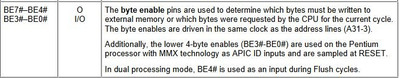
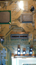
Tha additional capacitor is from BE7#to Vss?

Be7# to scyc if I’m looking at it right.

There is probably a definition for those pins somewhere if you wanted to look them up. Just leave it, prob something the board designers cooked up to resolve a defect
Edit: https://www.pchardwarelinks.com/586pin.htm
Yeah, idk what is going on there 🤣

Though it does get in the way of using a tweaker. You could still use one though, just have to desolder it and put it back on top.

Anyway, from what I can see,

You should be able to get 512mb of ram on this board

I’m not sure though if that tag chip supports caching that much ram though. Some of these mobos will give you a bios option for that.

But the caching is a non issue with k6-3/2+/3+ Because of its onboard cache.

If you want to use another processor you may be limited to 64mb of ram if that tag ram can’t cache the 512mb.

As for your cache, I’m assuming you have 512k? Can you confirm? that’s your max anyway. Chipset doesn’t support more.

Your max fsb is as I said 66mhz unfortunately. A limitation of your clock gen. But you might be able to replace the clock gen.

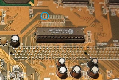
Your vrm looks like linear.

You should put a volt meter on the pin middle corner next to absent pin 1 to ground and play with your voltage jumpers. We need to know what voltages you can get there. It will tell us what cpus you can support. I suspect you’ll find a 2v or 2.2v setting. That will be sufficient.

As for multipliers, the tweaker can give you full access to all cpu supported multipliers on this mobo.

Finding working video cards for this mobo is challenging.

Many newer pci cards after geforce 4/5 stop working on 586 due to driver issues,

X800 series if they had made any pci cards for them (there is a x600 thing) but anyway it has a weird plug and dual gpus and is a mess, anway what I’m trying to say is you are looking at radeon 9000 series or geforce 4 series and below.

That cuts quite a few card out of the loop.

Next you probably need a card that works on 5v pci as most of these don’t have 3.3v

So again, more cards eliminated.

Next there is some other reason that seems to make 4 out of five cards you try not work in these.

However, there is one card that I’ve found that seems to work very well. Like seriously, I have a rage 128 that won’t even work. It’s so freakin picky

Low profile radeon 7500 pci.
Get one of those.

You can do radeon 7000 but it’s half as fast. Try to get the 7500
A close second is a radeon 9200 pro

As for sound, get a audigy 2 zs is the best performance wise probably also best quality.

You may have your preference for a isa card though but I’ve heard audigy 2zs can be made to work with dos. I know it works with 9x

As for storage: a promise sata II tx4 is a good investment for this board.

For your power supply, if you wanna use atx check out this:

ATX to AT pico Adapter! + Fan Headers Soft on/off, -5v, and 3.3v (Released)

Sphere's PCB projects.
-
Sphere’s socket 5/7 cpu collection.
-
SUCCESSFUL K6-2+ to K6-3+ Full Cache Enable Mod
-
Tyan S1564S to S1564D single to dual processor conversion (also s1563 and s1562)

Reply 23 of 240, by majestyk

User metadata
Rank Oldbie
Rank
Oldbie

Yeah - this is one of the boards maxing out onboard L2 cache with 512K but at the same time crippling the cacheable area to 64MB due to just one single onboard TAG chip. With 256K onboard and a COAST slot present there was a chance to add a 256K COAST module with an additional TAG onboard.
There are soldering pads for a SMD TAG chip and first I was afraid this might be just an alternative to the DIL TAG chip.
It depends on the wiring if this second TAG chip can add to the DIL one for all TAG lines to be activated.

tag-topic.JPG
Filename
tag-topic.JPG
File size
90.08 KiB
Views
793 views
File license
Public domain

I think the 3 additional datalines from the SMD pads go to the respective pins of the COAST (CELP) slot. So the pads were intended to be populated with an additional 128K TAG chip and using a COAST module with just 2 x 128K SRAM on it. Then, with 512K L2 in total and both TAG positions poopulated everything´s perfect.
You could buy a COAST module and the additional DIL TAG and be happy
The central question is if the layout provides the simultaneous use of both TAG-RAM positions when only onboard L2 is present.

Last edited by majestyk on 2022-05-28, 07:51. Edited 1 time in total.

Reply 24 of 240, by Sphere478

User metadata
Rank l33t++
Rank
l33t++

There may be a way to stack tags in one socket with a pcb and divorce the lines and run them boge wire to the needed pads or something similar.

In any case, if OP wants to use a k6 with onboard cache this becomes mostly irrelevant.

Sphere's PCB projects.
-
Sphere’s socket 5/7 cpu collection.
-
SUCCESSFUL K6-2+ to K6-3+ Full Cache Enable Mod
-
Tyan S1564S to S1564D single to dual processor conversion (also s1563 and s1562)

Reply 25 of 240, by majestyk

User metadata
Rank Oldbie
Rank
Oldbie

I recently tried this with my Jetway HX board. While soldering the stacked socket and wiring it the board died - probably dead HX northbridge due to ESD or something.
Since it´s BGA and I´m not very experienced in replacing those I decided to postpone this project.

Better go for some K6-II/III+ CPU...

Reply 26 of 240, by Sphere478

User metadata
Rank l33t++
Rank
l33t++
majestyk wrote on 2022-05-28, 07:57:

I recently tried this with my Jetway HX board. While soldering the stacked socket and wiring it the board died - probably dead HX northbridge due to ESD or something.
Since it´s BGA and I´m not very experienced in replacing those I decided to postpone this project.

Better go for some K6-II/III+ CPU...

Can you post schematics of what you were trying to do? Maybe a guide? Would love to read about it.

Just to clarify, there are three cpus that will help with this issue:

The k6-3
The k6-2+
And the k6-3+

No k6-2 cpus will help or any other cpu that will fit this mobo. Only those three types.

The + variant is the best and a 2+ can be modded to a 3+ sometimes (see signature) the + variant lets you change things from windows on the fly, and uses a smaller manufacturing process so uses less power.

Sphere's PCB projects.
-
Sphere’s socket 5/7 cpu collection.
-
SUCCESSFUL K6-2+ to K6-3+ Full Cache Enable Mod
-
Tyan S1564S to S1564D single to dual processor conversion (also s1563 and s1562)

Reply 27 of 240, by majestyk

User metadata
Rank Oldbie
Rank
Oldbie

I had started here:

The legendary HX chipset

Basically it´s all about activating the additional three I/O lines TIO 8 TIO 9 and TIO 10. TIO 0-7 are handeled by the first 128K TAG chip.
I carefully inspected some boards with two active TAG-chips and found that (besides Vss, Vcc and stuff) most of the data lines were wired parallel except that TIO 0 -TIO 7 are used on Chip 1 while 3 of the 8 I/O lines of Chip2 are connected to the 3 corresponding pins of the COAST slot AND the respective pins of the HX northbridge.
The problem with my Jetway board is that the TIO8-10 northbridge pins are not connected to any traces on the mainboard (because it has neither a CELP slot nor a second TAG socket) so I had to try to solder at the edge of the chip package.
This is not the case here, since there´s already 3 traces going to the CELP slot and we can be sure these in turn are already connected to the northbridge.

Quick and dirty: Take a second TAG chip, wire (nearly) everything in parallel to the first TAG chip, pick any 3 I/O lines and connect them to the 3 pins of the (unpopulated) CELP slot.

download/file.php?mode=view&id=123064

Last edited by majestyk on 2022-05-28, 12:15. Edited 1 time in total.

Reply 28 of 240, by Sphere478

User metadata
Rank l33t++
Rank
l33t++

So basically just solder two chips together except three pins? Bend them outward?, install the stack in the socket and use three boge wires to the coast slot? Pins 86 88 and 6?

That sounds super easy…

Sphere's PCB projects.
-
Sphere’s socket 5/7 cpu collection.
-
SUCCESSFUL K6-2+ to K6-3+ Full Cache Enable Mod
-
Tyan S1564S to S1564D single to dual processor conversion (also s1563 and s1562)

Reply 29 of 240, by majestyk

User metadata
Rank Oldbie
Rank
Oldbie

I hope it is. But probably this is exactly how "U28" on the Soyo board is wired.
Maybe 'CalamityLime' can make a closeup picture of this area with the DIL TAG chip pulled so we can guess better.

Reply 30 of 240, by CalamityLime

User metadata
Rank Member
Rank
Member

Hello.

Lots to read but just quickly reponding with images from my phone.

The tag ram is socketed. I could try taking the socket out if it helps.

Also the vrm looks to be switch mode to my eye. PNP transistors d45h2a. I would also suggest taking a quick look at the old fix up thread, in it i made a little fan mount that blows air across the CPU socket of my 486, this board will be going into the same case so it'll have the little fan blowing air across the VRM

Attachments

Be Happy, it's only going to get worse.
- Projects
Limes Strange 3D models
USB-2-232

Reply 31 of 240, by CalamityLime

User metadata
Rank Member
Rank
Member

Actually here's a different image without the harsh shadow.

Attachments

Be Happy, it's only going to get worse.
- Projects
Limes Strange 3D models
USB-2-232

Reply 33 of 240, by CalamityLime

User metadata
Rank Member
Rank
Member

The tag ram chip is a w24129ak-12, so that's a 16k tag ram i Believe.

The onboard cache chips are um61 3264f-7
Which seem to be 2megabit chips, there's two of them so that should be 512k onboard cache.
There's a jumper on board to switch between 256k and 512k and the jumper came set to 512, I'm guessing thats referring to the cache.

Be Happy, it's only going to get worse.
- Projects
Limes Strange 3D models
USB-2-232

Reply 34 of 240, by majestyk

User metadata
Rank Oldbie
Rank
Oldbie

This is the classic HX setup: 512K (2 x 32Kx8 or 4x 16Kx8) SRAM L2 cache and 2 x 128K (16Kx8) TAG RAM to make the full range of 512 MB RAM cacheable .

I see you have cleaned the solderings for the COAST socket. Are you planning to fit a socket in?

Reply 35 of 240, by CalamityLime

User metadata
Rank Member
Rank
Member
majestyk wrote on 2022-05-28, 13:17:

This is the classic HX setup: 512K (2 x 32Kx8 or 4x 16Kx8) SRAM L2 cache and 2 x 128K (16Kx8) TAG RAM to make the full range of 512 MB RAM cacheable .

I see you have cleaned the solderings for the COAST socket. Are you planning to fit a socket in?

I was thinking it could be fun to put a coast socket in there but it sounds like I don't need to.
Oh well, it gave me a good reason to finally clean out my solder sucker.

-Lime

Be Happy, it's only going to get worse.
- Projects
Limes Strange 3D models
USB-2-232

Reply 36 of 240, by LeFlash

User metadata
Rank Member
Rank
Member

I'd prefer to pull the other 5 data pins high or low permanently. Not parallel to the other chip, this only increases capacitance and maybe hurts due to different propagation delays between both rams.

Reply 37 of 240, by CalamityLime

User metadata
Rank Member
Rank
Member

Or we can make a PCB?

I threw this together just for the screen grab.

Attachments

Be Happy, it's only going to get worse.
- Projects
Limes Strange 3D models
USB-2-232

Reply 38 of 240, by CalamityLime

User metadata
Rank Member
Rank
Member

I'd also like to note in the thread that I had made a PCB to help with the RTC problem that I'm calling the DS1287-Hat

I guess I'll upload the files to github later, it's a really nice day here today so I want to head out somewhere and enjoy it.
But here are the images for that now if you want see it.

Attachments

Be Happy, it's only going to get worse.
- Projects
Limes Strange 3D models
USB-2-232

Reply 39 of 240, by majestyk

User metadata
Rank Oldbie
Rank
Oldbie
LeFlash wrote on 2022-05-28, 14:13:

I'd prefer to pull the other 5 data pins high or low permanently. Not parallel to the other chip, this only increases capacitance and maybe hurts due to different propagation delays between both rams.

100% agreed!

I just found the notes I took when examining a mainboard with 2 TAG-RAMS and transcribed it into the datasheet:

24129.JPG
Filename
24129.JPG
File size
74.09 KiB
Views
703 views
File license
Fair use/fair dealing exception

This is TAG-chip #1, the pins marked green are the ones wired parallel with the 2nd TAG-chip.
The red marked pins are for "T I/O 0-7" and lead directly to the CELP-slot contacts pin 2, 3, 4, 5, 82, 83, 84, 85 (if present) and to the HX northbridge.

TAG-chip #2 has the green pins connected to chip #1, pin 15-19 floating or pulled up or pulled down (I didn´t check) and pins 11, 12, 13 for T I/O 8, 9 and 10 are connected to the CELP-slot pins 6, 86 and 88 plus to the respective pins at the northbridge.

As for the SOYO board here, im 100% sure you could add the CELP-slot, populate it with a 256K cache stick, populate the SMD TAG-RAM and replace the two onboard 256K SRAM chips with two 128K chips and have a working setup. Maybe the unpopulated jumper at the CELP-slot would be needed.
All in all this sounds like a bummer to me since it´s a lot of work and there´s some risk the whole thing doesn´t work.

Alternatively you could just populate the SMD TAG-RAM and see if the cacheable area turns from 64MB to 512MB. Its cheaper, there´s very little risk and everything can be reverted easily.
If this works or not depends on weather the wiring of the mainboard fits for a situation with two 256K SRAMS onboard vs. the typical situation with 4 chips 128K each - 2 onboard and 2 on the COAST stick. I´m not sure about that.

And even situation 1 is confusing at first sight. Have a look at the SOYO version with the COAST slot populated:

Soyo_HX2.jpg
Filename
Soyo_HX2.jpg
File size
235.58 KiB
Views
699 views
File license
Fair use/fair dealing exception

The SMD TAG-chip is not present here. This means if the user upgrades the 256K onboard cache to 512K by adding a COAST stick the full cacheability depends on the COAST stick providing the second TAG-chip. And indeed many COAST sticks did have a TAG RAM at the time. Thil is probably the reason for the unpopulated SMD-TAG.
Note that JP24 is in position 1-2 here while it´s at 2-3 with no CELP-slot present.

Last edited by majestyk on 2022-05-28, 15:44. Edited 3 times in total.