There is another variant of the same board just with smaller onboard cache and the coast slot.
Are SMD tag ram chips available?
Even so would it not be more useful to experiment with making a tag ram pcb like i suggested above?
While if soldering on an SMD tag would be handy for me, making a PCB might be more useful for others with a HX board.
I was just adding the 2nd version while you were responding 😀
Fitting TAG chips are still available with 128K afaik.
The daughterboard variant clearly has it´s pros. You just would have to insert it and connect the three wires to the 3 COAST-slot pins. And others could use it also. Plus if you cannot get it to work just desolder 3 wires and remove the daughterboard.
I had made a prototype with vertically stacked chips for mainboards with little space, but I cannot find it right now.
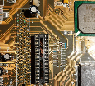
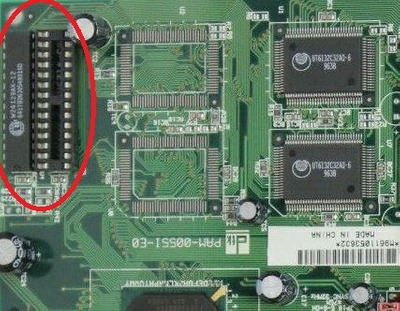
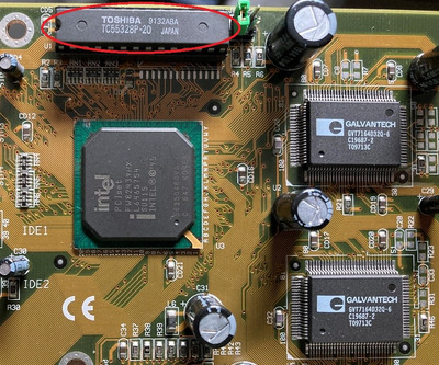
I buzzed out the cache connections on the 5TF some years ago. The two tag positions (DIP and SO) are connected to the same 8 tag bits (T0..T7), and these are also the only tag bits connected to the COAST slot. Looking at the traces emanating from the north bridge, I am very confident that the T8..T10 balls are not routed at all, thus negating one of the main selling points of the 430HX chipset.
THat´s a pity!
So they just implemented the old COAST standard with pins 6, 86 and 88 = NC, but packed 512K L2 cache on the board just for the PR-gag.
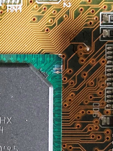
At least on the upper side there are no visible connections to these pins (green). And it slipped my eye that at the SMD pads all 7 I/O lines (green) are used which would be pointless if it was designed to act as additional TAG-RAM.
The SMD pads are only to be used for alternative (SMD) chips.
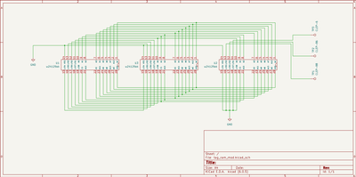
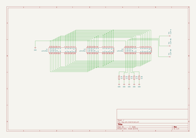
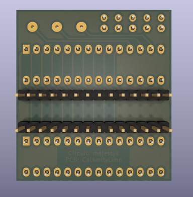
So following the instructions I layed out a circuit.
U1 is the first tag ram chip, U2 is the second tag ram chip and U3 is just the pin header to connect to the motherboard.
The Test points have their value set to the CLEP pin they go to.
Note: I did check the highlighted through hole pads 6 86 and 88 and they do not have a trace going to them.
Tis a shame but we could still make up a board and open source it. Maybe someone else would find it useful.
Did I miss something? I thought it was determined that you had enough bits on the one chip for 512mb cache?
I have one tag ram chip w24129ak-12, so that's a 16k X 8 bit.
Is that enough for the 512MB?
I suppose I should probably note that my want for this board to make something better than my 486 since testing the USB-2-232 was a little painful under windows 95, sometimes I was wondering if an issue was the machine being slow or my code being bad.
I'd just like something that can do maybe 98 with decent speeds plus decent dos support so I'm not swapping boards for any testing.
I don't really care about sound under DOS, the PC speaker and necrowares silly sound bastard are fun for me.
This is the classic HX setup: 512K (2 x 32Kx8 or 4x 16Kx8) SRAM L2 cache and 2 x 128K (16Kx8) TAG RAM to make the full range of 512 MB RAM cacheable .
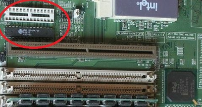
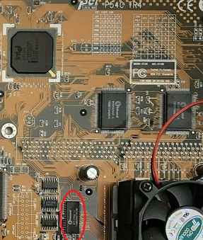
I see you have cleaned the solderings for the COAST socket. Are you planning to fit a socket in?
I’m trying to remember, I think you needed 11k or 12k of tag for 512mb which is why they often used 2x 8k chips? Because 16k chips weren’t a thing yet? I’m trying to remember, my memory os fuzzy on this.
I asked on discord, it was as I rembered, 11bits of tag and you are good to cache 512mb
Is it bits? Or kbits or kbites? I’m super rusty on this subject, but it seems if you have 16 of whatever it is, then you are good? As long as it’s using at least 11 of it.
When it comes to the TAG-RAM for a HX setup like this it´s not about the size / capacity of the TAG-RAM but about bus-width.
You could even have a 32Kx8 (256K) TAG-chip annd would still be limited to 64MB cacheable area due to the fact that when you are using just one chip you´re restricted to a 8-bit bus-witdh (=8 I/O lines). This means the whole TAG-bus of the northbridge that consists of 11 bus lines cannot be addressed.
To fulfill this condition you need to add a second TAG-RAM chip that takes care of the additional 3 I/O lines for a total 11-bit bus-width.
In an ideal world the board manufacturer makes sure the wiring makes this possible by
1. providing 2 sockets for TAG-chips
2. connecting all 11 I/O lines to the COAST-slot (if there is one) and - most important - to the northbridge.
- If only condition 1. is not met, the daughter-board solution will work, or, if there´s a COAST-slot present you can use a COAST-stick that brings it´s own additional TAG-chip
- If condition 2. is not met the problems begin, especially when the BGA-pins of the northbridge are not connected to any traces and cannot be reached.
Some manufaturers (like Jetway, Soyo, Aopen...) did a lousy job here by sparing the COAST-slot, sparing the second TAG-socket, sparing the second TAG-chip, just putting 2 x 256K SRAM on the boards and NOT changing the layout. This basically turns the cacheable area of HX back to FX.
The good (Gigabyte, ASUS, Chaintech, Elitegroup and others) did it right.
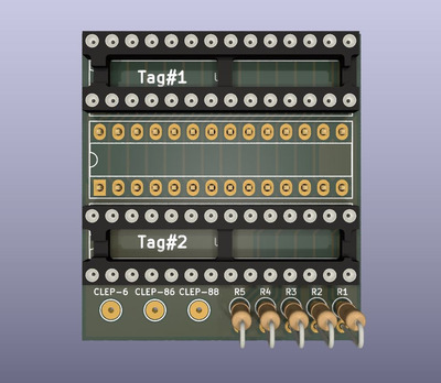
I can´t find any mistakes, maybe put a 1K resistor for pull down in each I/O line (I/O4-I/O8) at "U2".
I wanted to test my prototype on the Jetway board but I couldn´t, because of it´s early death so it´s all from what I measured when inspecting boards with a working 2-chip solution, but I can´t guarantee that I haven´t missed some connection...
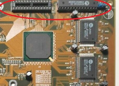
You can see in the Jetway picture above that I removed the coating on 2 traces at the upper-left corner of the HX BGA chip. While searching for the third one I had to get a wire as a probe under the chip and between the solder balls - this was probably the moment I damaged either some connection or triggered some ESD issue.
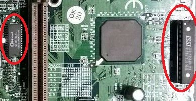
I measured the conductivity with a thin probe that reached the respective solder-balls underneath. This is possible for balls near the edge (1st or 2nd row), but the ball for the 3rd line lies deeper inside and is very hard to reach plus on this board there´s no unobstracted view from the side.
The soldering should be possible IF all three contacts have been identified. I´m not even sure if the third one is connected to a trace on the upper side at all.
Will this need bios support, or as soon as you connect all 11 bits of the bus you are good to go and the chipset does all the work?
Does making the tag larger kb wise have any benefit?
The 11-bit tag mode is a special option of the HX chipset that has to be enabled by the BIOS, using a bit in PCI configuration space (possibly it's strappable, I don't remember). I don't know whether typical HX BIOSes just blindly set this bit, or the board vendor has to customize the BIOS to enable that mode.
The number of required tag entries only depends on the cache size. You need one cache entry per cache line (16 bytes of cache on 486 boards, 32 bytes of cache on Pentium boards), so a 16k deep tag chip (e.g. 16k x 8 in a 128kbit chip) is good for 256KB / 512KB of cache, a 32k deep tag chip is good for 512KB / 1MB and a 64k deep tag chip enables 1MB on 486 systems or 2MB cache on Pentium system. Having tag RAM with more entries than required doesn't hurt (if the board can handle the chip), but doesn't yield any benefits.
Sorry for being quiet, something came up and hopefully it's over now.
I believe I am done with the tag ram board. I included the source files in this post.
I didn't know what to call it on the sheets so I just put in "HX Dual Tag Ram"