VOGONS


First post, by Ozzuneoj

User metadata
Rank l33t
Rank
l33t

Hello everyone. Long time no see!

I haven't really touched any retro PC stuff over the past year almost, but today I was looking through my CPUs and remembered that I had picked this gem up somewhere along the way a couple years ago, and I'd never really figured out exactly what it was.

I think it might be an Evergreen "386DX2+" upgrade chip, but it doesn't exactly match the PCB markings shown on this site.

https://www.ardent-tool.com/CPU/386_upgrade.html#386DX2+

... and I'll be honest and say that I don't really understand what the job of the adapter actually is. I have no interest in trying to pry this rare CPU out of the socket for more information, especially since the page above actually comments that a pin broke off while they did so for the picture (ouch!). That appears to be the only other picture of this upgrade chip on the internet, though I have found some pictures of the Ti SXL2-50 on it's own.

Can someone explain what I have here? What would it be used for that the SXL2-50 on it's own couldn't be used for?

Thanks!
Attachments

Now for some blitting from the back buffer.

Reply 2 of 17, by Ozzuneoj

User metadata
Rank l33t
Rank
l33t
Doornkaat wrote on 2022-11-19, 10:45:

Maybe an FPU?
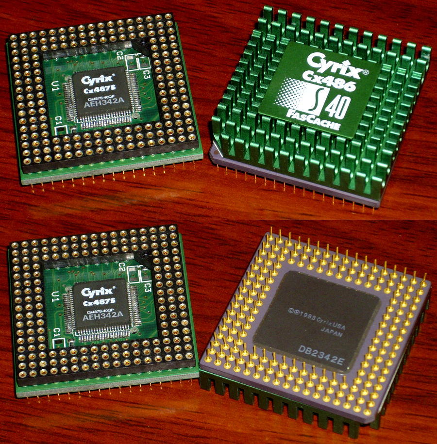
Had something similar before: Cyrix Cx486S with Cx487S FPU.

Sorry, I guess I should have clarified. I know what the chip itself is. It's basically a 386-compatible 486sx (no integrated FPU) with 8KB of L1 cache (a lot for a chip like this) that runs at 25mhz but can be internally clock-doubled to 50Mhz via a DOS utility. It is meant to drop into a standard 386 socket... So I'm unsure of what the stack of extra PCBs is doing.

I may have located something though...

https://www.cpu-world.com/forum/viewtopic.php?t=24350

Second post there says he has a similar chip that came attached to a voltage regulator of some kind? I'm not sure what the purpose is. I would definitely need to see a manual for this before trying to run it. I'd be gutted if I fried the thing because of incorrect voltage settings or something.

Edit: nevermind, I just noticed he said his is an smt chip on a PCB. Those are more common and are a different thing. What the heck is this? 😜

Now for some blitting from the back buffer.

Reply 3 of 17, by Sphere478

User metadata
Rank l33t++
Rank
l33t++

Re: Custom interposer module for TI486SXL2-66 PGA168 to PGA132 - HELP!

Cross linking

Sphere's PCB projects.
-
Sphere’s socket 5/7 cpu collection.
-
SUCCESSFUL K6-2+ to K6-3+ Full Cache Enable Mod
-
Tyan S1564S to S1564D single to dual processor conversion (also s1563 and s1562)

Reply 4 of 17, by Sphere478

User metadata
Rank l33t++
Rank
l33t++

Really curious to see where all those traces go.

Also if there are any components on the back side.

Unfortunately without seeing the traces and back of pcb, I’m not much help here.

Can you reconsider taking it apart? Be very careful if so. 😀

In the link, I’m not sure what that chip is on the back side. They don’t seem to say what it is, maybe a bus tranciever, maybe some configuration chip, kinda doubt that it is a math processor or cache, but maybe. It is 386 bus which is smaller pin set, but that still seems small.

Sphere's PCB projects.
-
Sphere’s socket 5/7 cpu collection.
-
SUCCESSFUL K6-2+ to K6-3+ Full Cache Enable Mod
-
Tyan S1564S to S1564D single to dual processor conversion (also s1563 and s1562)

Reply 6 of 17, by Ozzuneoj

User metadata
Rank l33t
Rank
l33t

I appreciate the interest guys.

Taking it apart will be my absolute last resort. Some of these CPUs have sold recently for upward of $400 without the unusual interposer\adapter. If someone that runs a site dedicated to things like this managed to break one disassembling it, I don't stand a chance. 😮

I just emailed the Ardent Tool site, just in case they can provide more information.

Now for some blitting from the back buffer.

Reply 7 of 17, by Doornkaat

User metadata
Rank l33t
Rank
l33t
Ozzuneoj wrote on 2022-11-19, 14:56:
Doornkaat wrote on 2022-11-19, 10:45:

Maybe an FPU?
Had something similar before: Cyrix Cx486S with Cx487S FPU.

I'm unsure of what the stack of extra PCBs is doing.

Yes. I mean there may be an FPU on the extra PCB like on the Cyrix Cx486S with Cx487S FPU combo I used to have.

SO-Cyrix-Cx487s-S40-FasCache.jpg
Image from CPU-world to clarify my previous post.

Reply 9 of 17, by Sphere478

User metadata
Rank l33t++
Rank
l33t++

If that is what it is, There’s a halfway decent chance my socket 1/2/3 tweaker could accomplish that also. (If someone else needed one)

I believe the pinouts of these is very similar to socket 1/2/3 for rhe pins in question such as power and feature pins

Socket 1/2/3 Voltage Interposer Tweaker (Alpha)

Pinouts between that CPU and standard socket 1/2/3 would have to be compared obv

Sphere's PCB projects.
-
Sphere’s socket 5/7 cpu collection.
-
SUCCESSFUL K6-2+ to K6-3+ Full Cache Enable Mod
-
Tyan S1564S to S1564D single to dual processor conversion (also s1563 and s1562)

Reply 10 of 17, by Ozzuneoj

User metadata
Rank l33t
Rank
l33t

I just got some very informative replies back from Tom at Ardent Tool. With his permission I'm posting them here.

The interposer pages were created by Tatsuo Sunagawa from Japan many many years ago. Some of his CPU upgrades and interposers ar […]
Show full quote

The interposer pages were created by Tatsuo Sunagawa from Japan many many years ago. Some of his CPU upgrades and interposers are now with me, but I'm not sure if the Evergreen 386DX2+ upgrade is among them. I can check later.

Anyway, looking at the photos, the side with the PGA plug seems pretty simple. Just some passives - bypass caps, pull-up/down or possibly configuration resistors.

The other side has only one component (aside from the socket) - a PQFP-44 IC. This is almost certainly some sort of PLD, with the sticker indicating the revision of the internal programming. What does this logic do? It's hard to tell for sure, but it likely modifies the behavior of some signals and/or reroutes them to improve compatibility (and make upgrading easier by eliminating jumpers/switches). These CPU interposers were aimed primarily at branded OEM systems rather than your cheapo clone boards. Many OEM boxes are rather picky about the CPU installed (timing of some signals, cache handling, etc.), so they might be compensating for some of that. Further, some interposers are designed to work in both - a regular 486 socket and the 487 upgrade socket with a slightly modified pinout. It's possible that the logic senses the socket type and reroutes the signals accordingly.

They might be also correcting for some errata/incompatibility in the TI CPU, though the interposer was probably used with different CPUs to provide different upgrade levels.

I don't see a voltage regulator so the SXL-40 must be a 5 V part.

We have some TI 486 datasheets here: https://ardent-tool.com/CPU/Docs_Other.html#TI

I can do some probing if I can find the interposer...

Cheers,
Tom

If I find the interposer I will do some probing to check what signals are passed through the programmable logic (and verify that it indeed is a PLD). That will tell us a lot about what's going on there. Some interposers even had internal registers addressable from software - but this was typically because of an on-board L2 cache controller - something that is almost certainly absent here.

Now for some blitting from the back buffer.

Reply 11 of 17, by Sphere478

User metadata
Rank l33t++
Rank
l33t++

Excellent! Sounds like we will have more answers soon!

Sphere's PCB projects.
-
Sphere’s socket 5/7 cpu collection.
-
SUCCESSFUL K6-2+ to K6-3+ Full Cache Enable Mod
-
Tyan S1564S to S1564D single to dual processor conversion (also s1563 and s1562)

Reply 12 of 17, by Ozzuneoj

User metadata
Rank l33t
Rank
l33t
Doornkaat wrote on 2022-11-19, 18:35:

Apparently my guess is wrong though.
http://www.amoretro.de/2013/01/386-clockdoubl … chensockel.html
This website describes it as a PCB necessary for the clock doubling feature to work.

Sorry, I missed this post earlier!

That is definitely the same as mine! Nice find!

Seems odd that it would be necessary to enable the clock doubler, because that is a feature of the CPU on it's own... Unless this device enables the clock doubler without the need for DOS utility tweaks as outlined in this video? Pretty neat if so.

EDIT: The one difference I see between the one at amoretro and mine is that mine has the intials "B.K." on it, where that one has "G.K."

Now for some blitting from the back buffer.

Reply 13 of 17, by kixs

User metadata
Rank l33t
Rank
l33t

I had this on my SXL2. I took it apart and used the CPU without it. I didn't find any differences in operation. I should still have a few of these adapters.

Requests are also possible... /msg kixs

Reply 14 of 17, by Ozzuneoj

User metadata
Rank l33t
Rank
l33t
kixs wrote on 2022-11-19, 23:21:

I had this on my SXL2. I took it apart and used the CPU without it. I didn't find any differences in operation. I should still have a few of these adapters.

Please send some pictures if you do have some of these. 😀

Also, regarding the amoretro link and the possibility of the interposer enabling clock doubling via hardware, Tom from Ardent Tools said:

It's possible, but features like that often default to disabled for a reason. Some POST routines may fail or give unexpected res […]
Show full quote

It's possible, but features like that often default to disabled for a reason. Some POST routines may fail or give unexpected results if the CPU runs too fast or has advanced features enabled (L2 cache, WB, etc.). And sometimes incompatibility exists on a hardware level...

I don't know enough about the TI CPU and can't tell from the photos where the PLD traces go. So I'm not gonna guess what exactly is its purpose.

Looks like the interposer from the link uses a different PLD (AMD PALCE 20V8H in a PLCC-28 package). Interesting...

Also, a correction to my previous comment - since this is a 386-compatible product, the 486/487 socket thing doesn't apply here.

Now for some blitting from the back buffer.

Reply 16 of 17, by Ozzuneoj

User metadata
Rank l33t
Rank
l33t

Wow! What is with that extra bit that wraps around it? That's about the craziest looking thing I've ever seen on a CPU.

Reminds me somewhat of the Socket 771 to 775 sticker mods that were popular 8-10 years ago... except those weren't on top of the chip.

I have read that the higher clocked 386>486 upgrade chips came with a cooler. I can't imagine it'd be easy to cool one with a flexible PCB wrapped around it.

Now for some blitting from the back buffer.

Reply 17 of 17, by kixs

User metadata
Rank l33t
Rank
l33t

I've no idea what that does. But it works like the ones without any adapter. I tested these chips on several motherboards. Some motherboards don't like the Ti486SXL and adapters doesn't matter.

Haven't seen one with the cooler. But they do get hot.

Requests are also possible... /msg kixs