VOGONS


First post, by majestyk

User metadata
Rank Oldbie
Rank
Oldbie

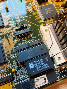
While flipping through the mainboards in my box of lost cases I came across an ASUS PCI/I-P5MP3, a nice old Socket 4 mainboard in very good condition and potentially working - if only the PAL near the CPU socket was present.

Asus_P5MP3_1.JPG
Filename
Asus_P5MP3_1.JPG
File size
1.18 MiB
Views
844 views
File license
Fair use/fair dealing exception

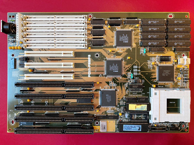
Originally I had the intention of buying a second and complete board and (try to) copy the PAL data from it. But these Socket 4 mainboards seem to have become collectors items and the last one on Ebay sold for a rediculous high price.
Since I´m not a reengineering genius I hope someone here has this board (in complete condition) and could dump the PAL´s data?

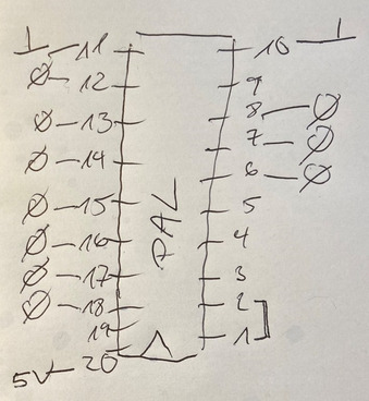
The sticker ASUS put on these DIL 20 chips says: IM3-G43-1
Hope someone can help!

Reply 3 of 17, by Roman555

User metadata
Rank Oldbie
Rank
Oldbie

There's an interesting blog how to dump a PAL especially if it's dump-protected.
Cloning a PAL/HAL , but all links to parts of the article are broken.
So I prefer it on web.archive.org - The Vintage Computer Forums - Chuck(G) - Blogs

[ MS6168/PII-350/YMF754/98SE ]
[ 775i65G/E5500/9800Pro/Vortex2/ME ]

Reply 4 of 17, by majestyk

User metadata
Rank Oldbie
Rank
Oldbie

I´m also wondering if ASUS protecded those PALs at that time.
But even if they did the way described in the VCF thread seems promising - provided that you have access to a working PAL.
On another blog they used "Logic Friday":
https://www.eevblog.com/forum/projects/lookin … tents-of-a-pal/

Edit:
I also tested the mainboard today just for fun. To my surprise at the very first start the POST display went through about 5 steps and then stopped at "43-something".
All following tests just produced "-- --".

Reply 5 of 17, by majestyk

User metadata
Rank Oldbie
Rank
Oldbie

After reflashing the BIOS chip, the board started without issues - and without PAL. The Turbo switch seems to have no effect.

But sometimes, after adding RAM or changing cache-configuration the BIOS gets corrupted and has to be reflashed to make the system start again. It´s not the chip, I tried two different ones.

P5MP3_speedsys.JPG
Filename
P5MP3_speedsys.JPG
File size
207.58 KiB
Views
723 views
File license
Public domain

I also measured all pins of the PAL socket for connectivity with the mainboard circuitry:

PAL_connect1.JPG
Filename
PAL_connect1.JPG
File size
99.98 KiB
Views
723 views
File license
Public domain

Pin 11 and 10 are grounded
Pin 20 is Vcc
Pins 1 and 2 are bridged and connected to the circuitry
Pins 3,4,5 and 19 are connected to the circuitry
Pins 6,7,8,12,13,14,15,16,17,18 are NC

The two questions at the moment are:
1. What´s the PAL needed for? Ìt seems like most outputs are not used.
2. Why is BIOS getting corrupted?

In the meantime I found a solution for the BIOS corruption issue. I replaced the (5V) Winbond Flash-ROM with an Intel P28F001BX-T, it needs 12V programming voltage(Vpp). The jumper JP12 is still in the 5V position (1-2). So far no further corruption incidents.

P5MP3_flashrom1.JPG
Filename
P5MP3_flashrom1.JPG
File size
503.55 KiB
Views
699 views
File license
Public domain

Reply 7 of 17, by majestyk

User metadata
Rank Oldbie
Rank
Oldbie

Pin 9 is connected also, I forgot it in the list.

I´ll try to trace down some connections. All the traces to/from the PAL are located in some inner PCB layers, which doesn´t make it easier.

PAL pin 19: -> pin U2 CPU socket = "FLUSH#" -> (H)

PAL pin 9: -> cold pin of the Turbo-LED connector and via a 33R to the hot pin of the Turbo Switch connector -> turbo switch closed (L), turbo switch open (H)

PAL pin 5: -> pin M3 CPU socket = "EADS#" ->(H)

PAL pin 4: -> pin L4 CPU socket = "BRDY#" -> (H)

PAL pin 3: -> pin P4 CPU socket = "ADS#" (then to S82434LX) -> (H)

PAL pin 1-2 -> pin 5 U44 (74F74) right besides the PAL -> (H)

Last edited by majestyk on 2022-11-30, 14:14. Edited 2 times in total.

Reply 9 of 17, by majestyk

User metadata
Rank Oldbie
Rank
Oldbie

This might well be.
They could have used the dual D-FlipFlop "74F74" as a frequency divider.

In this case I wouldn´t need the PAL, but on the other hand it would be a nice challenge to make the circuit work again.

Reply 10 of 17, by rasz_pl

User metadata
Rank l33t
Rank
l33t

I briefly looked at socket 5/7 schematics and at this stage chipsets seem to lack any slowdown functionality, looking at just two manuals for random boards with turbo headers suggests that they went for the most simplistic cache disable.
Access to BRDY (Burst Ready. If BRDY#=1, an external device needs more time = wait states) and FLUSH (L1 cache) pins would let Asus precisely tune slowdown to whatever they deemed necessary. On the other hand it could also be used to slow down IO to let CPU access something slow on the main bus. Whats with the separate flash chip, is it for storing https://en.wikipedia.org/wiki/Extended_System … figuration_Data ?

Open Source AT&T Globalyst/NCR/FIC 486-GAC-2 proprietary Cache Module reproduction

Reply 11 of 17, by majestyk

User metadata
Rank Oldbie
Rank
Oldbie

I switched the Vpp voltage for the BIOS Flash-ROM to 12V yesterday and it´s absolutely stable now when the hardware configuration changes. I wouldn´t be surprised if this board just doesn´t like certain BIOS chips.

The 430LX chipset also has a remarkable cacheable area of 192MB:

P5MP3_cache.JPG
Filename
P5MP3_cache.JPG
File size
132.83 KiB
Views
587 views
File license
Public domain

On most of the pictures I found on the web there´s a jumper on the Turbo-header, so "Turbo" seems to be enabled with the pins open.

Reply 13 of 17, by majestyk

User metadata
Rank Oldbie
Rank
Oldbie

The Turbo-jumper has no impact at all at the moment.

When L1 + L2 cache are disabled in BIOS speedsys CPU benchmark plummets from 45.49 to 8.16.

P5MP3_cache_dis.JPG
Filename
P5MP3_cache_dis.JPG
File size
167.38 KiB
Views
563 views
File license
Public domain

Reply 15 of 17, by majestyk

User metadata
Rank Oldbie
Rank
Oldbie

I attempted some more research today.
Pin 19 is the only active output of the PAL.

Two inputs of the PAL (1-2) are driven by the output (Q1) of the 74F74 dual FlipFlop.

At this FlipFlop:

CD# is "H" (Vcc)
SD# is "H" (Vcc)
CP is CPU clock (HCLKC)
D is "REFRESH" (ISA bus)

74F74_TT.JPG
Filename
74F74_TT.JPG
File size
17.48 KiB
Views
509 views
File license
Public domain

I wonder what we will see at the output Q?

Reply 17 of 17, by majestyk

User metadata
Rank Oldbie
Rank
Oldbie

According to the Intel documentation the 430LX-chipset does have a Turbo-Mode.
It´s called "De-Turbo Mode" assuming regular operation at full speed is Turbo-Mode.

LX_turbo.JPG
Filename
LX_turbo.JPG
File size
281.39 KiB
Views
457 views
File license
Public domain

This is of course about register values that can be set / changed by BIOS or by software - even at runtime. The Turbo pushbutton of an AT case cannot do this.
I will try and draw a diagram of what I have found so far about the circuitry around the PAL.