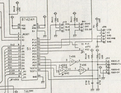
Pin 4 of the keyboard controller ("/RESET") is an active low reset signal. It may be high all the time, as it is active low. You might have trouble seeing a power-on reset on that signal when it's low for just 50ms after power on, but that would be fine. Pin 21 (CPU RESET, "P20") is an output signal that is again meant to be high all the time unless the CPU instructs the KBC to output a low pulse on that pin. So I don't think you have to worry about RESET for now.
If the CPU can't interface with the KBC, your issue might be on the low data bits D0 and D1 (they are used as "KBC ready" signals, pins 12 & 13), or on the /CS pin (pin 6), on the /RD or /WR pins (pin 8 and pin 10), or on the register select pin (pin 9). In a typical AT system, /RD is connected to ISA /IOR, /WR is connected to ISA /IOW, D0 and D1 may be connected to the ISA bus, but might also be on a different bus segment that is decoupled by driver chips. Usually, D0 and D1 of the keyboard controller is directly connected with D0 and D1 of the BIOS chip even if the ISA data pins and the KBC data pins are not connected. /CS is generated by the chipset on most 486 boards when address 60 or 64 is accessed. Some 486 chipsets use a combined chip select signal for the keyboard controller (responds only to I/O cycles) and the BIOS ROM (responds only to memory cycles). The register select pin is pin 2 of the I/O address, and should be connected to A2 on the ISA bus and/or A2 on the BIOS ROM chip.
Checking for a KBC clock (as Deunan suggested) is also a good idea. The KBC won't work unless a proper clock signal is present at pin 2. This signal can be generated from a central clock generator or using the internal oscillator driver of the KBC by connecting a crystal between pins 2 and 3. When the keyboard controller receives a valid clock on pin 2, it will output a clock signal on pin 3. Probing directly at pin 3 is a good way to check for a clock at the KBC without being afraid of loading the oscillator down so it stops oscillating.
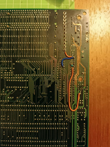
Verifying the connections I enumerated is a good idea to find broken traces/joints around the keyboard controller.