VOGONS


Reply 40 of 54, by mkarcher

User metadata
Rank l33t
Rank
l33t
majestyk wrote on 2023-03-11, 11:08:

Setting TAG-bit size from 8 (default) to 7 makes the difference in memory throughput performance in my case. When I set it to 7 the speedsys benchmarks are very similar to thoseCoffee One has:

I´m not sure what the reason is here, do you need 8-bit for larger RAM sizes? I only tested 64B (4 x 16M).

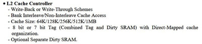
For L2 write-back cache to show sensible performance, you need to know whether the data in the L2 cache is newer than the data in the RAM (they call it "L2 cache is dirty"), so that when the cache should load other data, the chipset knows whether the old data from the cache needs to be written back to RAM, or it can simply be replaces. This requires one bit of storage for every data chunk in the cache ("cache line"). If you run L2 cache in write-back mode without storing this information, the chipset has to assume the worst case and always write the data from the cache back to main memory just at the moment the processor is stalled waiting for new data from the RAM to reach the processor. This operation mode is called "always dirty".

Old chipsets used a separate SRAM chip just to store the information whether a cache line is dirty (the "dirty bit" or "alter(ed) bit"). The RAM chip was called "dirty tag" or "alter tag". Modern 486 chipsets can combine the standard address tag (what has been stored in the tag RAM) and the "dirty"/"clean" information in the same 8-bit RAM chip. If you choose "TAG size: 8", the chipset uses all 8 bits for storing what part of memory is cached, and has no information about dirtyness. This is fine for L2 write-through, but causes the dreaded always-dirty mode in L2 write-back. This mode enables you to cache 64MB of RAM with 256KB of cache, 128MB of RAM with 512KB of cache or 256MB of RAM with 1MB of L2 cache. On the other hand, if you choose "TAG size: 7" (or "7+1", depending on your BIOS), only seven bits are used to know what part of memory is cached, and the eighth bit is used as "dirty"/"clean" indication. This allows sensible L2 write-back, but halves the amount of memory that can be cached.

The recommendation for genaral purpose computing is:

  1. Do not install more RAM than you L2 cache can cover (ctcm tests whether you have uncached memory).
  2. Do not use write-back mode without a dirty tag bit. If you need 8 bits for the address tag, switch L2 to write-through mode.
  3. If seven tag bits are enough, write-back is preferrable over write-through.

If you have the skills/tools to set aside the uncached part of RAM for "non-performance critical operation" like a RAM drive, you may install more RAM than L2 cache covers (violating the first recommendation), but if you know how to do that, you likely would have written this answer yourself 😀

Reply 41 of 54, by majestyk

User metadata
Rank Oldbie
Rank
Oldbie

According to the datasheet a seperate "dirty SRAM" chip is supported. I wonder if this could be added some way?

85C496_cc.JPG
Filename
85C496_cc.JPG
File size
29.97 KiB
Views
708 views
File license
Public domain

In the meantime I upgraded to 512K L2 and 32Kx8 TAG.
There was a 16Kx8 TAG chip present for the 256K version that should have been 32Kx8 according to the manual.

64MB RAM are competely cacheable now and the memory throughput is at 46.1 MB/s. So for 64MB it´s all right as it seems.

486SPM_speeds512.JPG
Filename
486SPM_speeds512.JPG
File size
188.33 KiB
Views
708 views
File license
Public domain

Reply 42 of 54, by jakethompson1

User metadata
Rank Oldbie
Rank
Oldbie
majestyk wrote on 2023-03-11, 18:17:

According to the datasheet a seperate "dirty SRAM" chip is supported. I wonder if this could be added some way?
85C496_cc.JPG

There are some 486 chipsets that support neither write-through chipsets nor robbing one bit of the tag as the dirty bit. The UM491 is one, and I have a board that uses it and omits the dirty SRAM (and doesn't even provide a socket for it) so it's stuck in an Always Dirty configuration.

User PC-Engineer has written in the past about hacking a board to add the dirty RAM when none was provided for, by using a "piggyback" configuration to stick another chip on top the Tag RAM such that the only address bits + Vcc/GND get connected through to the new tag RAM. Then wires get run to connect the correct pins on the chipset through to the replacement "dirty" RAM. Re: 486 cache/ram speed issue with write-back

Something I don't understand is that x1 SRAMs have separate pins for data in and out, while x8 SRAMs have "bidirectional" pins, so if the chipset has separate dirty-in and dirty-out pins, as the UM491 does, (but I thought I saw one that did?) is it safe to short them together in order to (ab)use a piggybacked x8 SRAM as if it were a x1 dirty SRAM.

To be clear since your chipset supports 7+1, at the cost of halving the cacheable area (512KB could cache 128MB, and 1MB could cache 256MB, if there is a dedicated dirty bit), there is absolutely no performance advantage to providing the dedicated dirty bit unless you have too much memory and need to enlarge the cacheable area.

Reply 43 of 54, by mkarcher

User metadata
Rank l33t
Rank
l33t
jakethompson1 wrote on 2023-03-11, 22:28:
majestyk wrote on 2023-03-11, 18:17:

According to the datasheet a seperate "dirty SRAM" chip is supported. I wonder if this could be added some way?
85C496_cc.JPG

There are some 486 chipsets that support neither write-through chipsets nor robbing one bit of the tag as the dirty bit. The UM491 is one, and I have a board that uses it and omits the dirty SRAM (and doesn't even provide a socket for it) so it's stuck in an Always Dirty configuration.

I have a 386DX40 board in a similar configuration. I'm still undecided whether I will leave it that way to preserve the original state (as I know that the previous owner of that board values "pristine state"), or I will add the dirty tag (including lifting the pin that is supposed to be connected to "dirty out") to get a top notch 386 system. It's a shame that those chipsets do not provide write-through for low-cost boards that omit the dirty SRAM.

jakethompson1 wrote on 2023-03-11, 22:28:

Something I don't understand is that x1 SRAMs have separate pins for data in and out, while x8 SRAMs have "bidirectional" pins, so if the chipset has separate dirty-in and dirty-out pins, as the UM491 does, (but I thought I saw one that did?) is it safe to short them together in order to (ab)use a piggybacked x8 SRAM as if it were a x1 dirty SRAM.

Most likely it is not safe. There is a point in the dedicated data-in/data-out configuration: You do not need any controls for making sure there is no conflict on who is driving the data line(s). This simplifies chip construction and can relax some timing requirements, especially in read-modify-write operations, as read data and write data is transferred through different channels. On the other hand, there also is a point in the combined in/out configuration: Pins are a scarce resource! Building ICs with less pins is cheaper. That's why x1 chips usually have dedicated in and out pins (that extra pin doesn't hurt much), but you have combined data in/out on x4 and x8 chips (which would require 4 or 8 extra pins).

Not only the pins on the SRAMs are a scarce resource, but the pins at the chipset are, too, often even more so. If the chipset designer could save one pin by providing a single dirty I/O pin instead of two separate dirty pins, the designer most likely will have chosen that route. So most likely any chipset that has the dedicated dirty in/dirty out pins has a simple push/pull (aka totem pole) output driver on the pin used to write the dirty bit, and connecting that pin to the data out pin of the SRAM will cause a bus conflict.
[/quote]

Reply 44 of 54, by mkarcher

User metadata
Rank l33t
Rank
l33t
majestyk wrote on 2023-03-11, 18:17:

According to the datasheet a seperate "dirty SRAM" chip is supported. I wonder if this could be added some way?

(citing the SiS 85c496 data sheet)

Like most 486 chipset manufacturers, SiS ran out of pins, and you need to chose a limited set of features, you can't have all at once. The separate SRAM uses at least two extra pins (DIRTYWE and DIRTY). These functions are not available in all configurations. IIRC they content with with MA11 (required to support 64MB and 128MB PS/2 SIMMs) and one of the PCIREQ/PCIGNT pairs (one pair required per master-capable PCI slot). If you want to add the extra SRAM, you likely need to adjust your BIOS to initialize the chipset into a configuration that exposes DIRTYWE and DIRTY, and you likely have to lift pins to free them from their old purpose and add bodges to connect them to the dedicated dirty SRAM. There is a table in the datasheet that explains the interoperation of the configuration bits.

Reply 45 of 54, by CoffeeOne

User metadata
Rank Oldbie
Rank
Oldbie
majestyk wrote on 2023-03-11, 18:17:
According to the datasheet a seperate "dirty SRAM" chip is supported. I wonder if this could be added some way? 85C496_cc.JPG […]
Show full quote

According to the datasheet a seperate "dirty SRAM" chip is supported. I wonder if this could be added some way?
85C496_cc.JPG

In the meantime I upgraded to 512K L2 and 32Kx8 TAG.
There was a 16Kx8 TAG chip present for the 256K version that should have been 32Kx8 according to the manual.

64MB RAM are competely cacheable now and the memory throughput is at 46.1 MB/s. So for 64MB it´s all right as it seems.
486SPM_speeds512.JPG

Yes, optimal performance.

Reply 46 of 54, by jakethompson1

User metadata
Rank Oldbie
Rank
Oldbie
mkarcher wrote on 2023-03-11, 23:49:

I have a 386DX40 board in a similar configuration. I'm still undecided whether I will leave it that way to preserve the original state (as I know that the previous owner of that board values "pristine state"), or I will add the dirty tag (including lifting the pin that is supposed to be connected to "dirty out") to get a top notch 386 system. It's a shame that those chipsets do not provide write-through for low-cost boards that omit the dirty SRAM.

Intel has a nice write-up about designing a cache to fit an 80386 from November 1986 (https://www.dropbox.com/sh/sj97ghb5jqbpahe/AA … er+1985.300.pdf page 24). It's a nice overview of how caches work overall too. In it, they suggest that write-back (or as they call it, deferred write), "...requires much more logic, allows the DRAM to contain stale data (the cache is more up-to-date than the DRAM), and generally does not in­crease overall system performance unless a heavily accessed dual-port DRAM is used." So I wonder why chipset manufacturers, if they had to support only one or the other, decided to support only write-back rather than only write-through.

Reply 47 of 54, by mkarcher

User metadata
Rank l33t
Rank
l33t
jakethompson1 wrote on 2023-03-12, 00:09:

Intel has a nice write-up about designing a cache to fit an 80386 from November 1986 (https://www.dropbox.com/sh/sj97ghb5jqbpahe/AA … er+1985.300.pdf page 24). It's a nice overview of how caches work overall too. In it, they suggest that write-back (or as they call it, deferred write), "...requires much more logic, allows the DRAM to contain stale data (the cache is more up-to-date than the DRAM), and generally does not in­crease overall system performance unless a heavily accessed dual-port DRAM is used." So I wonder why chipset manufacturers, if they had to support only one or the other, decided to support only write-back rather than only write-through.

That Intel statement was state of the art in 1986. We are talking about chipsets from around 1993. That's seven years of rapidly increasing integration, so "much more logic" isn't an issue in 1993, while it was a big issue in 1986. "Allows DRAM to contain stale data" is only a point if DMA is accessing DRAM without going through the L2 cache. Intel proposed caches architectures with the L2 being "in between" the processor and the remaining system, so the L2 and processor could be combined on a single "processor module". In a design like that, DMA would sidestep the processor module and hit the DRAM directly. But that's not how 1993 486 chipsets for the consumer market were designed. The SRAM-based cache is not to be seen as "attached to the processor", but as "attached to the RAM". Everything that accesses RAM will use L2 cache, so it doesn't matter that RAM might be stale. Having DMA sidestep a cache is a complicated situation, especially solving the problem in an efficient way. We experienced the problems Intel was talking about when L1WB got common: As L1 is integrated into the processor, L1WB always implies a setup with DMA on the "memory side" of the cache, not the "processor side".

Properly implemented write-back caches (WITH dirty bits) do increase system performance, even without dual-port DRAM. I guess Intel refers to the issue that a dirty cache line is flushed while the processor already is stalled on reading data, so the write-back process will actively hurt system performance, and this deficit has to be overcompensated by writes caught by the cache that don't go through to the DRAM. Dual-ported DRAM systems could perform the write-back process in parallel with the fill process to overcome this issue. It seems that cache implementation techniques also improved between 1986 and 1993, making write-back more viable.

Write-back cache was a marketable feature, that's why "supports writeback L2 cache" was an important feature to have on the banner specs of the chipset. As WB/WT selectable is more difficult than WB only, a cheap chipset that supports WB (due to marketing demands) might not support WT, as it would increase complexity and thus both research & development cost as well as production cost.

Reply 48 of 54, by Masejoer

User metadata
Rank Newbie
Rank
Newbie

What AH4 revision is your board, majestyk? I have a 1.1 AH4T here that doesn't have headers in some positions, but soldered jumpers. It's also an AMI BIOS, and refuses to POST with a p71-133 CPU, with POST code 23. DX4-100 works fine, although the AMI BIOS has no setting to change the L2 cache to 7+1. Overall this board as it sits is pretty bad, with poor memory bandwidth and no p75-133 support.

You mentioned setting a couple jumpers where I don't have any headers located - I would need to solder headers in those permanently-jumpered spots, and it sounds like a switch to an Award BIOS may be in order.

Reply 49 of 54, by majestyk

User metadata
Rank Oldbie
Rank
Oldbie

My board is revision 1.1, but note it came without VRM so I had to add some components.
You can see the jumpering for 5x86 CPUs here on the pic from page 1:

AB_AH4_jump_final2.jpg
Filename
AB_AH4_jump_final2.jpg
File size
580.23 KiB
Views
594 views
File license
Fair use/fair dealing exception

All the blue coloured jumpers had to be added or changed.
When running a 5x86 CPU I would suggest you use Jan´s AWARD BIOS. He posted a download link earlier in this thread.

Reply 50 of 54, by Masejoer

User metadata
Rank Newbie
Rank
Newbie
majestyk wrote on 2023-04-10, 06:09:
My board is revision 1.1, but note it came without VRM so I had to add some components. You can see the jumpering for 5x86 CPUs […]
Show full quote

My board is revision 1.1, but note it came without VRM so I had to add some components.
You can see the jumpering for 5x86 CPUs here on the pic from page 1:
AB_AH4_jump_final2.jpg

All the blue coloured jumpers had to be added or changed.
When running a 5x86 CPU I would suggest you use Jan´s AWARD BIOS. He posted a download link earlier in this thread.

Yeah, for example, I don't have headers for JP10. Pins 2-3 are factory soldered with a wire. There are a few positions on my board where it came with soldered bridges, rather than jumpers. AB-AH4T v1.1, and the factory CPU regulator outputs 3.45V, not 3.3 per the manual. Good for a 5x86-133, but no successful POST in stock form.

It's interesting that your v1.1 board is so different, even starting life as a non-T variant.

Edit:
Never mind, I see in your first photo that you also had soldered bridges. I didn't see that mentioned, but saw headers in the later photos.

Reply 52 of 54, by Masejoer

User metadata
Rank Newbie
Rank
Newbie
majestyk wrote on 2023-04-10, 06:25:

I thought the AH4T was full featured and only the AH4 was crippled. Strange they even limited the AH4T in some ways so 5x86 use is disabled.

The low-Voltage components missing as labeled in your first post are indeed different (AH4T 1.1 has them), but the other parts of the board all appear to be the same. Mine appeared never used when I got it, and everything has been very tight trying to change factory-default jumpers, add expansion cards, and even using the socket mechanism.

Won't stay like-new though - it needs some changes to get better functionality. Even though the battery looks original and like it has never received power, it needs to come off too so it won't corrode later, although it appears to have charged up fine at first power on. It's half the size of yours, but the solder looks original.

Reply 53 of 54, by Masejoer

User metadata
Rank Newbie
Rank
Newbie

It's too bad that I can't stick with an AMI BIOS on this thing - still POST code 23 with the 5x86-133 . Also no way to set 7+1 on the L2, or set to write-through. My own nostalgia with a 486 includes the AMI WinBIOS, so it's my own preference on socket 3. I'll wait for some W27C512 to arrive to flash with AWARD.

I added pin headers to the spots on the mainboard. I only get POST code A5 when I try to change any of those new jumpers to anything that isn't the factory jumpered locations. All headers have been verified as having continuity further along the traces/test points, so the headers are soldered fine.