Masejoer wrote on 2023-03-28, 07:15:
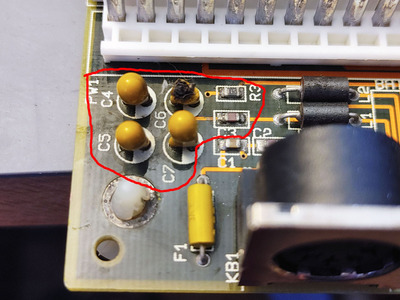
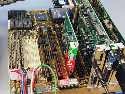
I have a Freetech 486F30 or Genoa TURBOEXPRESS 486VL motherboard here that is stalling out on POST (no display) with code 08. AMI BIOS. Motherboard had light corrosion where the battery was, but cleaned up well and all the traces appear to be intact. I can follow AT pins 2, 3, 4, and 5 to the keyboard controller chip. I am unable to find where pin 1/clock goes. I don't get anything from pin1 to the keyboard controller, or any pins on the SiS chips.
You should double-check that you are counting the pins in the right way. Only four pins on the AT connector are supposed to be connected. Pin 3, originally a RESET signal for XT keyboards, is typically unconnected. The actual clock pin should be connected to Pin 1 of the keyboard controller.
Masejoer wrote on 2023-03-28, 07:15:
I was just looking at this area due to the battery corrosion and because AMI 08 says "BAT command to keyboard controller is issued, and "CMOS checksum started."
Not only the connections between the keyboard controller and the keyboard are suspect after battery leakage, but the connections between the keyboard controller and the chipset are suspect, too. Designers of PC/XT/AT BIOSes usually have in mind that something on the keyboard connection might be fishy, as it is an external connection, and programmed their system accordingly. On the other hand, distrust into the mainboard itself during POST was still a thing in the PC/XT days (the BIOS checked that all 8 data bits were actually functional on the PIC, the PIT, the DMA controller), but testing that stuff declined over the years. This decline makes sense, as most of those peripheripherals got integrated into a single chip, the ubiquitious 82C206, initially designed by C&T, but cloned by every chipset maker. Data lines inside a chip don't tend to break or have bad contact in the socket.
In the case of the AT keyboard controller, the BIOS needs to synchronize with the microcode inside the keyboard controller. For that to work, the keyboard controller needs to be executing its microcode (that is, it needs to get a valid clock signal), and furthermore the 8 data bits, the chip select, the register select and the read and write command lines need to be connected from the chipset to the keyboard controller. The issue you are facing hint to a communication problem between the processor and the keyboard controller.
In many boards, the keyboard controller and the BIOS chip have their data lines connected. Testing continuity between D0-D7 of the KBC to D0-D7 of the ROM BIOS are a good initial check for the data bits. Furthermore, the read and write line of the KBC are likely directly tied to ISA /IOR and ISA /IOW - another easy continuity measurement can confirm this. The register select line of the keyboard controller is supposed to be connected to address line A2, which can be shared with A2 on the BIOS ROM, A2 on the ISA bus, or both of them.
Masejoer wrote on 2023-03-28, 07:15:
I'm not sure where to go from here in troubleshooting the board. The BIOS chip is cleaned and I have used deoxit to make sure things are making good contact.
If you get that far into the POST, you can be confident that all the data pins and the chip select logic of the BIOS chip is working fine. A missing address bit on the BIOS chip might be possible, but is unlikely in my experience. I would postpone investigating the BIOS chip until you have excluded communication issues between the chipset and the KBC, which tends to be the culprit of issues like this more often.
Masejoer wrote on 2023-03-28, 07:15:
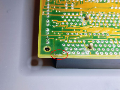
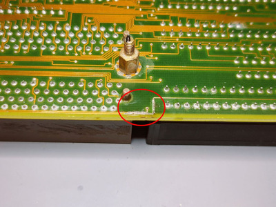
Everything else ohm-meter tests fine in the area of the AT connector/removed battery, besides not knowing how to follow the AT clock pin (no surface traces on bottom or top of the board - it goes into a middle layer).
The usual layer configuration of consumer 486 boards is a 4-layer configuration that only has +5V and GND on the inner layers. Some boards use a 6-layer configuration, but on most of those baords, the power planes are still in the center of the board (planes 3 and 4), and the space between 1 and 2, as well as 5 and 6 is so small that you can see traces on all of those four layers. So a valid rule of thumb is: If you can't see a trace on either side of the board (and that's not just because there is a component blocking you to look at the top side), that pin is connected to ground, to +5V or completely unconnected.