First post, by Jamieson

Rank
Newbie
- Rank
- Newbie
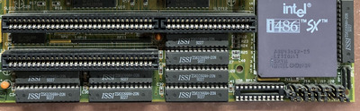
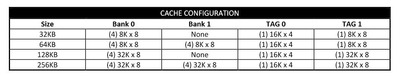
I have the 486 motherboard "SIH 486B" from NIC Technology. It seems to be properly configured for 64kB cache with 8 x 8Kx8 cache chips installed, TAG1 is 8Kx8, but TAG0 is empty. According to the datasheet TAG0 should be 16Kx4 in all cache configurations. Motherboard reports 64KB cache at POST. In benchmarks see a drop in memory read performance at 64KB so it looks like the cache is doing something, yet cachechk does not think there is any L2 cache in this 486SX-25 system. The two pictures of this motherboard on retroweb also show the TAG0 socket is empty. Does this seem normal for a dual TAG cache configuration?
https://theretroweb.com/motherboards/s/nic-te … gy-inc-sih-486b