VOGONS


First post, by WJG6260

User metadata
Rank Member
Rank
Member

Hello all!

I've been messing with this Daewoo AL486D, Revision 1.1 motherboard, which came out of a Leading Edge PC I own.

I took the motherboard out the case for testing and noticed something quite odd: The VLB slot farthest from the CPU, at the bottom of the board, seems not to work with a VLB VGA card. A VLB VGA card placed in the first slot, closest to the CPU, works fine.

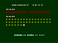
I used a POST diagnostic card to see what was going on, and it appears that the board hangs on post code 2C when a VLB VGA card is placed in the second slot/farthest slot, which indicates "video ROM check" is the point at which failure occurs.

The PC was originally equipped with a Trident 8900D ISA card, so I couldn't help but wonder if this was some sort of manufacturing issue, but I have sort of ruled that out via the testing methodology shared below.

I've tried all the usual suspects to narrow down a reason for this and first attempted the following:

  • Booting with two 8-bit and 16-bit ISA VGAs in the farthest slot, which in both cases does work as anticipated
  • Clearing the CMOS--Note that this board lacks a CMOS battery onboard, so all testing sessions result in new settings anyway
  • Testing other VLB card (a known good S3 928-based Number Nine GXE and a known good S3 805i-based Acer OEM card), which resulted in the same
  • Testing with other VLB cards (S3 805i-based Acer OEM card), which also resulted intermittently in non-detection of the VGA card and beeps indicative of such
  • Testing/replacing the tantalum caps between the bottom two ISA slots (a few of them were indeed bad, measuring as short circuits on my multimeter and confirmed on a cheapo ESR meter)
  • Testing/replacing the resistor networks between the two VLB slots, as one seemed to test suspicious/bad (although in-circuit testing is not really helpful, I still wanted to give this a go)
  • Trying other 386DX and 486DLC CPUs, besides the TI 486SXL-40 pictured
  • Probing each and every VLB pin with an oscilloscope, which yielded activity on all address/data lines, and normal 5v/GND signals
  • Continuity testing seems fine with a DMM. I can't find any broken traces either
  • Trying to fiddle with the VLB-specific jumpers on this board

I've bolded this last point because, after replacing the tantalum caps and resistor networks, I could boot with a VLB VGA card in the second slot if and only if I had the VLB jumpers set appropriately; this board seemed picky, insofar as at 40MHz FSB, I needed to set the jumper to >33MHz FSB. No wait states were needed with any cards I used.

Problem solved? Nope.

After setting the board aside for a bit, it is back to its original antics of rarely--if at all--POSTing with a VLB VGA in the bottom slot. The same 2C POST code as before is present during these times.

I suspected cold solder joints, so I reflowed the entire VLB slot and added fresh solder to each and every joint by hand. I also reflowed the CPU slot, and did the same there. This did not change anything.

A pertinent question I have is this: Are any VLB-specific address pins used for decoding the VGA BIOS? I would have thought that this would have occurred on the ISA side of things, but wouldn't I have a problem with an ISA VGA card in that case? On another board I have, I found two address pins were disconnected between two slots, rendering four ISA slots incapable of running 16-bit VGA cards. I discovered this because an 8-bit ISA VGA card worked in those slots, so I fixed the issue with a couple of small bodge wires. The same doesn't seem to be the case here, as ISA VGAs of all types work just fine in this farthest/second slot.

I'm about ready to replace the whole darned VLB slot, as I have a few extra slots and have done this before. I just was wondering if there's anything else I might be missing. I'm ripping my hairs out over this and feeling somewhat neurotic because I cannot, for the life of me, find anything wrong.

Does anyone have any thoughts? Thanks in advance!

Attached are some higher-res pics of the board.

Board front view:
AFGJ81qC-IIXnwnVi9QU-ayMwyGIbU_CdQMmqcwCTOfhRP0GyWUHQatjkkvik7TWPogtsjLqMl3ZJ-vp7d1duSQjIW4mJNXH-g=s1600

Board rear view (I probably should do a better job cleaning the flux, but if I'm gonna replace the darned slot I'll leave it for now I guess...):
AFGJ81ptvaDdU6oNi0uF7HjmEftfRdQxPdq_ztjcD-tNEs_N2UTOk3o4x_NKziE6yGkdZ3_nEGVclmbywCJzW0eBPtn4VnKunA=s1600

2C POST halt when VLB is in secondary slot:
AFGJ81pBEm8_abHmU7RS1E7qqOM-lyUqN9cZXTDIKkarpuuEekT2c0txRxMdOi9I5wD9qrTOzckt0kj1RsbP8vPIhidtDDwJ7g=s1600

Normal POST when VLB VGA is in first slot (pic is mid-boot, so ignore the missing digit):
AFGJ81pFKiKemDiTGJreOOVgaSTdqBdeKrUmf4Xo4Afcp0J85jZ3JoXZKnVwWnbYf0NS-E6LEjgBCI16eHWI4HPNupwh3yDLew=s1600

Last edited by WJG6260 on 2023-06-30, 01:40. Edited 2 times in total.

-Live Long and Prosper-

Feel free to check out my YouTube and Twitter!

Reply 3 of 22, by kixs

User metadata
Rank l33t
Rank
l33t

On my board the VGA card works fine on all VLB slots.

What about other VLB cards - I/O - do they work? I noticed on some VLB motherboards that VGA won't work but I/O works.

Requests are also possible... /msg kixs

Reply 5 of 22, by WJG6260

User metadata
Rank Member
Rank
Member
Disruptor wrote on 2023-06-28, 04:53:

On a local bus VGA card all the communication with its BIOS runs through the ISA part of the card.

This makes sense, and I kind of figured that by looking at the traces on my Trio64. I guess the issue lies elsewhere then? Maybe in a ready signal of some kind or perhaps in a case where there’s one joint under the slot that’s cracked or something?

I can’t figure out why this slot works just fine with ISA 8/16-bit VGAs but struggles with VLB cards.

Potentially a dumb question: Do you (or does anyone) know if there’s a book/manual/datasheet somewhere that describes VLB VGA initialization routines? I’m wondering if it’s an issue at a step right before the BIOS ROM is read.

pshipkov wrote on 2023-06-28, 06:49:

I would go with multimeter and check if each two corresponding pins between the two slots are connected. Can be something simple as cold joint.

I mentioned this issue to Feipoa and he was the one who informed me as to how important/picky the board is about the VLB jumpers.

I’ve checked every point between the VLB pins for continuity and even compared with another ALi M1429 board. I went ahead and reflowed and rechecked the pins anyway, as well.

The only thing of note that I suppose there was reared its head in resistance testing. There was 20 kOhms between the two slots on pins A49, A50, and A52, but 40 kOhms on this board. I’m inclined to believe that’s not the whole picture and not the issue, but I could be wrong.

kixs wrote on 2023-06-28, 06:39:

On my board the VGA card works fine on all VLB slots.

What about other VLB cards - I/O - do they work? I noticed on some VLB motherboards that VGA won't work but I/O works.

Feipoa shared this too.

Have you also noticed that this board is particular when it comes to the VLB FSB jumper? I found it to be super picky, when things were working.

I’ve been able to get I/O going in the farthest slot, but I don’t see why such—and not a VGA—would work. I didn’t test an I/O card with a BIOS. I may do this later and see if there’s anything there; I’d be even more confused if that was the case solely because there’s no issues with ISA VGAs working.

-Live Long and Prosper-

Feel free to check out my YouTube and Twitter!

Reply 6 of 22, by Disruptor

User metadata
Rank Oldbie
Rank
Oldbie
WJG6260 wrote on 2023-06-28, 13:35:

Potentially a dumb question: Do you (or does anyone) know if there’s a book/manual/datasheet somewhere that describes VLB VGA initialization routines? I’m wondering if it’s an issue at a step right before the BIOS ROM is read.

Basically you can boot from a monochrome graphics card and initialise the VGA BIOS through DOS' debug.

Reply 7 of 22, by WJG6260

User metadata
Rank Member
Rank
Member
Disruptor wrote on 2023-06-28, 13:41:
WJG6260 wrote on 2023-06-28, 13:35:

Potentially a dumb question: Do you (or does anyone) know if there’s a book/manual/datasheet somewhere that describes VLB VGA initialization routines? I’m wondering if it’s an issue at a step right before the BIOS ROM is read.

Basically you can boot from a monochrome graphics card and initialise the VGA BIOS through DOS' debug.

Interesting. I don’t have a monochrome card or monitor off-hand but I’d be willing to try this if swapping the slot doesn’t change anything. That was my “last resort” anyway.

-Live Long and Prosper-

Feel free to check out my YouTube and Twitter!

Reply 8 of 22, by mkarcher

User metadata
Rank l33t
Rank
l33t

The best way to debug the issue without a monochrome card is to set up serial debugging. Pull the ROM from the VL card (you need to do that anyway to prevent the POST to lock up, even with an MDA installed), ignore the beep code that there is no valid graphics card. Have the BIOS image in a file, and load it using DEBUG. DEBUG will load the image as is it were a COM file, which is is not. So you need to adjust CS to be 10 higher than it is, and then set IP to 3, and you can start stepping through the initialization routine.

I expect that some cycle that accesses the S3 chip will lock up the local bus, possibly because a trace on the VL bus is broken, or a contact in the lower VL slot is bad. For example, if the card recognizes a cycle, it activates the "LDEV" signal to tell the chipset that this cycle is going to be handled by the VL card. When the VL card is done handling the cycle, it will activate the "LRDY" signal. Suppose the LRDY signal is broken: In that case, the processor/chipset will wait indefinite time for the end of the cycle.

Reply 9 of 22, by WJG6260

User metadata
Rank Member
Rank
Member
mkarcher wrote on 2023-06-28, 19:05:

The best way to debug the issue without a monochrome card is to set up serial debugging. Pull the ROM from the VL card (you need to do that anyway to prevent the POST to lock up, even with an MDA installed), ignore the beep code that there is no valid graphics card. Have the BIOS image in a file, and load it using DEBUG. DEBUG will load the image as is it were a COM file, which is is not. So you need to adjust CS to be 10 higher than it is, and then set IP to 3, and you can start stepping through the initialization routine.

I expect that some cycle that accesses the S3 chip will lock up the local bus, possibly because a trace on the VL bus is broken, or a contact in the lower VL slot is bad. For example, if the card recognizes a cycle, it activates the "LDEV" signal to tell the chipset that this cycle is going to be handled by the VL card. When the VL card is done handling the cycle, it will activate the "LRDY" signal. Suppose the LRDY signal is broken: In that case, the processor/chipset will wait indefinite time for the end of the cycle.

Ah, okay, this makes sense. I was wondering if something like this would work. I’m not too familiar with DEBUG commands, but I found a template of sorts from a prior thread about initializing a VGA card manually with the BIOS still in the card. A different situation, surely, I suppose things would have to be changed to meet your suggestions. The pertinent lines seem to be:

debug
a
call c000:3
int 20
(enter)
g
q

If you don’t mind, I have a few questions about your DEBUG suggestion. I presume CS is code segment, so “10 higher than it is” would be C010 then? Not to sound amateurish, but after reading some, I presume IP=3 would set the IP to 3, then? I guess the question is this: What do I need to change to run debug and get things loaded from a file named, e.g., s3.bin?

I guess One last question is this, if you don’t mind: How would I step through the initialization if I cannot see the screen? Would I need to use a separate VGA card? Or could this be done in AUTOEXEC.BAT?

Thanks for the information about LDEV and LRDY! This makes a lot of sense. I suppose that’s why it seems like there’s a ROM issue but, since the ISA-side of things seems okay, it’s probably to do with the VLB slot. I suppose that, if this method of debugging works, and it turns out to be the slot/traces/something of that sort, I’ll go ahead and do the physical repairs.

Thanks again for this suggestion! I will try this once I understand what steps to take and then report back here. 😀

-Live Long and Prosper-

Feel free to check out my YouTube and Twitter!

Reply 10 of 22, by Disruptor

User metadata
Rank Oldbie
Rank
Oldbie

wait, i explain "serial debugging":

use a zero modem cable, initialize COM1 with mode and redirect DOS' input and output via ctty command (in autoexec.bat)
use a serial console on a laptop nearby, like every hacker does 😄

Reply 11 of 22, by jakethompson1

User metadata
Rank Oldbie
Rank
Oldbie
WJG6260 wrote on 2023-06-28, 20:15:

If you don’t mind, I have a few questions about your DEBUG suggestion. I presume CS is code segment, so “10 higher than it is” would be C010 then? Not to sound amateurish, but after reading some, I presume IP=3 would set the IP to 3, then? I guess the question is this: What do I need to change to run debug and get things loaded from a file named, e.g., s3.bin?

He is saying to load the VGA BIOS from a .COM file on disk, not try to debug the "live" VGA BIOS at c000:0. You can't set a breakpoint in ROM so you'd be limited to tracing one instruction at a time rather than being able to go until a certain address, "proceed" to step over function calls etc.

When you debug a .COM file, it loads it at cs:100h because the program segment prefix is the first 100h bytes in the segment. By bumping up the segment by 10h, you advance the linear address by 100h, canceling that out and putting your COM file at cs:0, so that cs:3 is then the entry point of the VGA BIOS.

Reply 12 of 22, by WJG6260

User metadata
Rank Member
Rank
Member
Disruptor wrote on 2023-06-28, 20:52:

wait, i explain "serial debugging":

use a zero modem cable, initialize COM1 with mode and redirect DOS' input and output via ctty command (in autoexec.bat)
use a serial console on a laptop nearby, like every hacker does 😄

OH! This makes so much sense. Thank you @Disruptor. I’ve done this many times and never once thought it had an actual name 🤣

jakethompson1 wrote on 2023-06-28, 21:30:
WJG6260 wrote on 2023-06-28, 20:15:

If you don’t mind, I have a few questions about your DEBUG suggestion. I presume CS is code segment, so “10 higher than it is” would be C010 then? Not to sound amateurish, but after reading some, I presume IP=3 would set the IP to 3, then? I guess the question is this: What do I need to change to run debug and get things loaded from a file named, e.g., s3.bin?

He is saying to load the VGA BIOS from a .COM file on disk, not try to debug the "live" VGA BIOS at c000:0. You can't set a breakpoint in ROM so you'd be limited to tracing one instruction at a time rather than being able to go until a certain address, "proceed" to step over function calls etc.

When you debug a .COM file, it loads it at cs:100h because the program segment prefix is the first 100h bytes in the segment. By bumping up the segment by 10h, you advance the linear address by 100h, canceling that out and putting your COM file at cs:0, so that cs:3 is then the entry point of the VGA BIOS.

@jakethompson1

Ah, okay. I see! I’ve never even remotely attempted something of this sort.

Is there a basic guide for this? I really hate to sound clueless/helpless, but I have to admit when things are a little above me.

As far as the address, that makes sense to me. I guess it’s just the process of actually doing this that’s confusing me somewhat.

Sorry to @all for the myriad questions, but I do want to try this and see how it goes!

-Live Long and Prosper-

Feel free to check out my YouTube and Twitter!

Reply 13 of 22, by mkarcher

User metadata
Rank l33t
Rank
l33t
Disruptor wrote on 2023-06-28, 20:52:

use a zero modem cable, initialize COM1 with mode and redirect DOS' input and output via ctty command (in autoexec.bat)

The way to do that is

mode com1:9600,n,8,1
ctty com1

You should test these commands with a working graphics card (like your Trident card). To get back to control your computer locally, use "ctty con" on the serial terminal.

Of course, the terminal should be set to the same parameters, i.e. 9600 baud, 8 data bits, 1 stop bit, no parity. If your serial terminal is a windows computer, putty is a good choice for a terminal program.

jakethompson1 wrote on 2023-06-28, 21:30:

He is saying to load the VGA BIOS from a .COM file on disk, not try to debug the "live" VGA BIOS at c000:0. You can't set a breakpoint in ROM so you'd be limited to tracing one instruction at a time rather than being able to go until a certain address, "proceed" to step over function calls etc.

When you debug a .COM file, it loads it at cs:100h because the program segment prefix is the first 100h bytes in the segment. By bumping up the segment by 10h, you advance the linear address by 100h, canceling that out and putting your COM file at cs:0, so that cs:3 is then the entry point of the VGA BIOS.

Exactly. Furthermore, as the ROM has been removed from the card, it can't be accessed at C000:0 any more, unless you hot-plug it back. Loading it from a file is easier, and having it in RAM allows for breakpoints, as you say.
Here is a (made-up) example session:

C:\>debug s3.bin
-rcs
CS 14a3
:14b3
-rip
IP 0100
3
-r
AX=0000 BX=0000 CX=0000 DX=0000 SP=FFEE BP=0000 SI=0000 DI=0000
DS=14A3 ES=14A3 SS=14A3 CS=14B3 IP=0003 NV UP EI PL NZ NA PO NC
14B3:0003 E9 5B 00 JMP 0061
-t
AX=0000 BX=0000 CX=0000 DX=0000 SP=FFEE BP=0000 SI=0000 DI=0000
DS=14A3 ES=14A3 SS=14A3 CS=14B3 IP=0003 NV UP EI PL NZ NA PO NC
14B3:0061 .... ........
-q
C:\>

The debug command, rcs, modifies CS. You need to add 10 (hex) to the value displayed. If you are completely unfamiliar with hexadecimal arithmetic, use your favorite calculator program, put it into "programmer" mode or something like that, and switch it to "hex" or "base 16". The second debug command, rip, modifies IP, setting it from 0100 (the starting offset for COM programs) to 0003 (the starting offset for ROM BIOS initialization functions. The subsequent r command is used to perform a basic validation that you didn't mess up the previous commands. The instruction at the entry point of a ROM is almost always a jump instruction. If you don't see a jump instruction, something went wrong.

Please consult a debug tutorial or intro video on YouTube on details about how to step with debug. A complete introduction into debug is more work than I can provide on this forum.

Reply 14 of 22, by WJG6260

User metadata
Rank Member
Rank
Member
mkarcher wrote on 2023-06-28, 22:41:
The way to do that is […]
Show full quote
Disruptor wrote on 2023-06-28, 20:52:

use a zero modem cable, initialize COM1 with mode and redirect DOS' input and output via ctty command (in autoexec.bat)

The way to do that is

mode com1:9600,n,8,1
ctty com1

You should test these commands with a working graphics card (like your Trident card). To get back to control your computer locally, use "ctty con" on the serial terminal.

Of course, the terminal should be set to the same parameters, i.e. 9600 baud, 8 data bits, 1 stop bit, no parity. If your serial terminal is a windows computer, putty is a good choice for a terminal program.

jakethompson1 wrote on 2023-06-28, 21:30:

He is saying to load the VGA BIOS from a .COM file on disk, not try to debug the "live" VGA BIOS at c000:0. You can't set a breakpoint in ROM so you'd be limited to tracing one instruction at a time rather than being able to go until a certain address, "proceed" to step over function calls etc.

When you debug a .COM file, it loads it at cs:100h because the program segment prefix is the first 100h bytes in the segment. By bumping up the segment by 10h, you advance the linear address by 100h, canceling that out and putting your COM file at cs:0, so that cs:3 is then the entry point of the VGA BIOS.

Exactly. Furthermore, as the ROM has been removed from the card, it can't be accessed at C000:0 any more, unless you hot-plug it back. Loading it from a file is easier, and having it in RAM allows for breakpoints, as you say.
Here is a (made-up) example session:

C:\>debug s3.bin
-rcs
CS 14a3
:14b3
-rip
IP 0100
3
-r
AX=0000 BX=0000 CX=0000 DX=0000 SP=FFEE BP=0000 SI=0000 DI=0000
DS=14A3 ES=14A3 SS=14A3 CS=14B3 IP=0003 NV UP EI PL NZ NA PO NC
14B3:0003 E9 5B 00 JMP 0061
-t
AX=0000 BX=0000 CX=0000 DX=0000 SP=FFEE BP=0000 SI=0000 DI=0000
DS=14A3 ES=14A3 SS=14A3 CS=14B3 IP=0003 NV UP EI PL NZ NA PO NC
14B3:0061 .... ........
-q
C:\>

The debug command, rcs, modifies CS. You need to add 10 (hex) to the value displayed. If you are completely unfamiliar with hexadecimal arithmetic, use your favorite calculator program, put it into "programmer" mode or something like that, and switch it to "hex" or "base 16". The second debug command, rip, modifies IP, setting it from 0100 (the starting offset for COM programs) to 0003 (the starting offset for ROM BIOS initialization functions. The subsequent r command is used to perform a basic validation that you didn't mess up the previous commands. The instruction at the entry point of a ROM is almost always a jump instruction. If you don't see a jump instruction, something went wrong.

Please consult a debug tutorial or intro video on YouTube on details about how to step with debug. A complete introduction into debug is more work than I can provide on this forum.

Thank you so much! This makes a lot of sense. I managed to test out accessing the MS-DOS command line via serial perfectly using my main PC and a USB->Serial converter.

I see where having breakpoints is ideal for debugging. This also makes a lot of sense.

Over dinner, I read into the debug syntax and watched a video or two; I kind of see what's going on here now. I am familiar with hex as well, so no problem there; thanks for simplifying things though, especially for any future readers with similar issues.

---
Since the board has no mono/color jumper, I set the AMIBIOS to a video card type of "Not Installed." I also disabled ROM shadowing for the VGA BIOS, not that such matters since the EPROM was removed anyway. I then proceeded to test the system with the card in the working slot. I ran rcs, and received a value of 1349, and modified it to 1359. Setting IP to 3 and running -r, I saw JMP 0009, which makes sense. I stepped through the whole .bin file, and reached the end where it looped into a LOADSW. Not that I claim to know VGA BIOSes, but from my knowledge of assembly, I suppose that makes sense given what goes on in the background.

I put the card in the bad slot and repeated the process. The terminal/system hung after stepping through to the following instruction:

OUT DX,AL

The whole debug output was as follows (sorry it's so long!):

debug s3.bin
-rcs
CS 1349
:1359
-rip
IP 0100
:3
-r
AX=0000 BX=0000 CX=8000 DX=0000 SP=FFEE BP=0000 SI=0000 DI=0000
DS=1349 ES=1349 SS=1349 CS=1359 IP=0003 NV UP EI PL NZ NA PO NC
1359:0003 EB04 JMP 0009
-t

AX=0000 BX=0000 CX=8000 DX=0000 SP=FFEE BP=0000 SI=0000 DI=0000
DS=1349 ES=1349 SS=1349 CS=1359 IP=0009 NV UP EI PL NZ NA PO NC
1359:0009 E9B61F JMP 1FC2
-t

AX=0000 BX=0000 CX=8000 DX=0000 SP=FFEE BP=0000 SI=0000 DI=0000
DS=1349 ES=1349 SS=1349 CS=1359 IP=1FC2 NV UP EI PL NZ NA PO NC
1359:1FC2 FA CLI
-t

AX=0000 BX=0000 CX=8000 DX=0000 SP=FFEE BP=0000 SI=0000 DI=0000
DS=1349 ES=1349 SS=1349 CS=1359 IP=1FC3 NV UP DI PL NZ NA PO NC
1359:1FC3 60 DB 60
-t

AX=0000 BX=0000 CX=8000 DX=0000 SP=FFDE BP=0000 SI=0000 DI=0000
DS=1349 ES=1349 SS=1349 CS=1359 IP=1FC4 NV UP DI PL NZ NA PO NC
1359:1FC4 06 PUSH ES
-t

AX=0000 BX=0000 CX=8000 DX=0000 SP=FFDC BP=0000 SI=0000 DI=0000
DS=1349 ES=1349 SS=1349 CS=1359 IP=1FC5 NV UP DI PL NZ NA PO NC
1359:1FC5 1E PUSH DS
-t

AX=0000 BX=0000 CX=8000 DX=0000 SP=FFDA BP=0000 SI=0000 DI=0000
DS=1349 ES=1349 SS=1349 CS=1359 IP=1FC6 NV UP DI PL NZ NA PO NC
1359:1FC6 83EC02 SUB SP,+02
-t

AX=0000 BX=0000 CX=8000 DX=0000 SP=FFD8 BP=0000 SI=0000 DI=0000
DS=1349 ES=1349 SS=1349 CS=1359 IP=1FC9 NV UP DI NG NZ NA PE NC
1359:1FC9 FC CLD
-t

AX=0000 BX=0000 CX=8000 DX=0000 SP=FFD8 BP=0000 SI=0000 DI=0000
DS=1349 ES=1349 SS=1349 CS=1359 IP=1FCA NV UP DI NG NZ NA PE NC
1359:1FCA 8BEC MOV BP,SP
-t

AX=0000 BX=0000 CX=8000 DX=0000 SP=FFD8 BP=FFD8 SI=0000 DI=0000
DS=1349 ES=1349 SS=1349 CS=1359 IP=1FCC NV UP DI NG NZ NA PE NC
1359:1FCC 2E CS:
1359:1FCD 8E1EBC1F MOV DS,[1FBC] CS:1FBC=0000
-t

AX=0000 BX=0000 CX=8000 DX=0000 SP=FFD8 BP=FFD8 SI=0000 DI=0000
Show last 263 lines
DS=0000  ES=1349  SS=1349  CS=1359  IP=1FD1   NV UP DI NG NZ NA PE NC
1359:1FD1 B80112 MOV AX,1201
-t

AX=1201 BX=0000 CX=8000 DX=0000 SP=FFD8 BP=FFD8 SI=0000 DI=0000
DS=0000 ES=1349 SS=1349 CS=1359 IP=1FD4 NV UP DI NG NZ NA PE NC
1359:1FD4 B332 MOV BL,32
-t

AX=1201 BX=0032 CX=8000 DX=0000 SP=FFD8 BP=FFD8 SI=0000 DI=0000
DS=0000 ES=1349 SS=1349 CS=1359 IP=1FD6 NV UP DI NG NZ NA PE NC
1359:1FD6 CD10 INT 10
-t

AX=1201 BX=0032 CX=8000 DX=0000 SP=FFD2 BP=FFD8 SI=0000 DI=0000
DS=0000 ES=1349 SS=1349 CS=068D IP=18B3 NV UP DI NG NZ NA PE NC
068D:18B3 9C PUSHF
-t

AX=1201 BX=0032 CX=8000 DX=0000 SP=FFD0 BP=FFD8 SI=0000 DI=0000
DS=0000 ES=1349 SS=1349 CS=068D IP=18B4 NV UP DI NG NZ NA PE NC
068D:18B4 2E CS:
068D:18B5 FE06B923 INC BYTE PTR [23B9] CS:23B9=00
-t

AX=1201 BX=0032 CX=8000 DX=0000 SP=FFD0 BP=FFD8 SI=0000 DI=0000
DS=0000 ES=1349 SS=1349 CS=068D IP=18B9 NV UP DI PL NZ NA PO NC
068D:18B9 FA CLI
-t

AX=1201 BX=0032 CX=8000 DX=0000 SP=FFD0 BP=FFD8 SI=0000 DI=0000
DS=0000 ES=1349 SS=1349 CS=068D IP=18BA NV UP DI PL NZ NA PO NC
068D:18BA 2E CS:
068D:18BB FF1EC423 CALL FAR [23C4] CS:23C4=F065
-t

AX=1201 BX=0032 CX=8000 DX=0000 SP=FFCC BP=FFD8 SI=0000 DI=0000
DS=0000 ES=1349 SS=1349 CS=F000 IP=F065 NV UP DI PL NZ NA PO NC
F000:F065 E9D2A3 JMP 943A
-t

AX=1201 BX=0032 CX=8000 DX=0000 SP=FFCC BP=FFD8 SI=0000 DI=0000
DS=0000 ES=1349 SS=1349 CS=F000 IP=943A NV UP DI PL NZ NA PO NC
F000:943A FB STI
-t

AX=1201 BX=0032 CX=8000 DX=0000 SP=FFCC BP=FFD8 SI=0000 DI=0000
DS=0000 ES=1349 SS=1349 CS=F000 IP=943B NV UP EI PL NZ NA PO NC
F000:943B FC CLD
-t

AX=1201 BX=0032 CX=8000 DX=0000 SP=FFCC BP=FFD8 SI=0000 DI=0000
DS=0000 ES=1349 SS=1349 CS=F000 IP=943C NV UP EI PL NZ NA PO NC
F000:943C 80FC0E CMP AH,0E
-t

AX=1201 BX=0032 CX=8000 DX=0000 SP=FFCC BP=FFD8 SI=0000 DI=0000
DS=0000 ES=1349 SS=1349 CS=F000 IP=943F NV UP EI PL NZ AC PO NC
F000:943F 7440 JZ 9481
-t

AX=1201 BX=0032 CX=8000 DX=0000 SP=FFCC BP=FFD8 SI=0000 DI=0000
DS=0000 ES=1349 SS=1349 CS=F000 IP=9441 NV UP EI PL NZ AC PO NC
F000:9441 80FC02 CMP AH,02
-t

AX=1201 BX=0032 CX=8000 DX=0000 SP=FFCC BP=FFD8 SI=0000 DI=0000
DS=0000 ES=1349 SS=1349 CS=F000 IP=9444 NV UP EI PL NZ NA PO NC
F000:9444 743E JZ 9484
-t

AX=1201 BX=0032 CX=8000 DX=0000 SP=FFCC BP=FFD8 SI=0000 DI=0000
DS=0000 ES=1349 SS=1349 CS=F000 IP=9446 NV UP EI PL NZ NA PO NC
F000:9446 80FC03 CMP AH,03
-t

AX=1201 BX=0032 CX=8000 DX=0000 SP=FFCC BP=FFD8 SI=0000 DI=0000
DS=0000 ES=1349 SS=1349 CS=F000 IP=9449 NV UP EI PL NZ AC PE NC
F000:9449 743C JZ 9487
-t

AX=1201 BX=0032 CX=8000 DX=0000 SP=FFCC BP=FFD8 SI=0000 DI=0000
DS=0000 ES=1349 SS=1349 CS=F000 IP=944B NV UP EI PL NZ AC PE NC
F000:944B 80FC05 CMP AH,05
-t

AX=1201 BX=0032 CX=8000 DX=0000 SP=FFCC BP=FFD8 SI=0000 DI=0000
DS=0000 ES=1349 SS=1349 CS=F000 IP=944E NV UP EI PL NZ AC PO NC
F000:944E 743A JZ 948A
-t

AX=1201 BX=0032 CX=8000 DX=0000 SP=FFCC BP=FFD8 SI=0000 DI=0000
DS=0000 ES=1349 SS=1349 CS=F000 IP=9450 NV UP EI PL NZ AC PO NC
F000:9450 60 DB 60
-t

AX=1201 BX=0032 CX=8000 DX=0000 SP=FFBC BP=FFD8 SI=0000 DI=0000
DS=0000 ES=1349 SS=1349 CS=F000 IP=9451 NV UP EI PL NZ AC PO NC
F000:9451 1E PUSH DS
-t

AX=1201 BX=0032 CX=8000 DX=0000 SP=FFBA BP=FFD8 SI=0000 DI=0000
DS=0000 ES=1349 SS=1349 CS=F000 IP=9452 NV UP EI PL NZ AC PO NC
F000:9452 06 PUSH ES
-t

AX=1201 BX=0032 CX=8000 DX=0000 SP=FFB8 BP=FFD8 SI=0000 DI=0000
DS=0000 ES=1349 SS=1349 CS=F000 IP=9453 NV UP EI PL NZ AC PO NC
F000:9453 80FC13 CMP AH,13
-t

AX=1201 BX=0032 CX=8000 DX=0000 SP=FFB8 BP=FFD8 SI=0000 DI=0000
DS=0000 ES=1349 SS=1349 CS=F000 IP=9456 NV UP EI NG NZ AC PE CY
F000:9456 7725 JA 947D
-t

AX=1201 BX=0032 CX=8000 DX=0000 SP=FFB8 BP=FFD8 SI=0000 DI=0000
DS=0000 ES=1349 SS=1349 CS=F000 IP=9458 NV UP EI NG NZ AC PE CY
F000:9458 50 PUSH AX
-t

AX=1201 BX=0032 CX=8000 DX=0000 SP=FFB6 BP=FFD8 SI=0000 DI=0000
DS=0000 ES=1349 SS=1349 CS=F000 IP=9459 NV UP EI NG NZ AC PE CY
F000:9459 8AC4 MOV AL,AH
-t

AX=1212 BX=0032 CX=8000 DX=0000 SP=FFB6 BP=FFD8 SI=0000 DI=0000
DS=0000 ES=1349 SS=1349 CS=F000 IP=945B NV UP EI NG NZ AC PE CY
F000:945B 98 CBW
-t

AX=0012 BX=0032 CX=8000 DX=0000 SP=FFB6 BP=FFD8 SI=0000 DI=0000
DS=0000 ES=1349 SS=1349 CS=F000 IP=945C NV UP EI NG NZ AC PE CY
F000:945C 8BF8 MOV DI,AX
-t

AX=0012 BX=0032 CX=8000 DX=0000 SP=FFB6 BP=FFD8 SI=0000 DI=0012
DS=0000 ES=1349 SS=1349 CS=F000 IP=945E NV UP EI NG NZ AC PE CY
F000:945E B84000 MOV AX,0040
-t

AX=0040 BX=0032 CX=8000 DX=0000 SP=FFB6 BP=FFD8 SI=0000 DI=0012
DS=0000 ES=1349 SS=1349 CS=F000 IP=9461 NV UP EI NG NZ AC PE CY
F000:9461 8ED8 MOV DS,AX
-t

AX=0040 BX=0032 CX=8000 DX=0000 SP=FFB6 BP=FFD8 SI=0000 DI=0012
DS=0040 ES=1349 SS=1349 CS=F000 IP=9463 NV UP EI NG NZ AC PE CY
F000:9463 7410 JZ 9475
-t

AX=0040 BX=0032 CX=8000 DX=0000 SP=FFB6 BP=FFD8 SI=0000 DI=0012
DS=0040 ES=1349 SS=1349 CS=F000 IP=9465 NV UP EI NG NZ AC PE CY
F000:9465 A01000 MOV AL,[0010] DS:0010=30
-t

AX=0030 BX=0032 CX=8000 DX=0000 SP=FFB6 BP=FFD8 SI=0000 DI=0012
DS=0040 ES=1349 SS=1349 CS=F000 IP=9468 NV UP EI NG NZ AC PE CY
F000:9468 2430 AND AL,30
-t

AX=0030 BX=0032 CX=8000 DX=0000 SP=FFB6 BP=FFD8 SI=0000 DI=0012
DS=0040 ES=1349 SS=1349 CS=F000 IP=946A NV UP EI PL NZ AC PE NC
F000:946A 3C30 CMP AL,30
-t

AX=0030 BX=0032 CX=8000 DX=0000 SP=FFB6 BP=FFD8 SI=0000 DI=0012
DS=0040 ES=1349 SS=1349 CS=F000 IP=946C NV UP EI PL ZR NA PE NC
F000:946C B800B0 MOV AX,B000
-t

AX=B000 BX=0032 CX=8000 DX=0000 SP=FFB6 BP=FFD8 SI=0000 DI=0012
DS=0040 ES=1349 SS=1349 CS=F000 IP=946F NV UP EI PL ZR NA PE NC
F000:946F 7402 JZ 9473
-t

AX=B000 BX=0032 CX=8000 DX=0000 SP=FFB6 BP=FFD8 SI=0000 DI=0012
DS=0040 ES=1349 SS=1349 CS=F000 IP=9473 NV UP EI PL ZR NA PE NC
F000:9473 8EC0 MOV ES,AX
-t

AX=B000 BX=0032 CX=8000 DX=0000 SP=FFB6 BP=FFD8 SI=0000 DI=0012
DS=0040 ES=B000 SS=1349 CS=F000 IP=9475 NV UP EI PL ZR NA PE NC
F000:9475 58 POP AX
-t

AX=1201 BX=0032 CX=8000 DX=0000 SP=FFB8 BP=FFD8 SI=0000 DI=0012
DS=0040 ES=B000 SS=1349 CS=F000 IP=9476 NV UP EI PL ZR NA PE NC
F000:9476 D1E7 SHL DI,1
-t

AX=1201 BX=0032 CX=8000 DX=0000 SP=FFB8 BP=FFD8 SI=0000 DI=0024
DS=0040 ES=B000 SS=1349 CS=F000 IP=9478 NV UP EI PL NZ NA PE NC
F000:9478 2E CS:
F000:9479 FF951294 CALL [DI+9412] CS:9436=9B47
-t

AX=1201 BX=0032 CX=8000 DX=0000 SP=FFB6 BP=FFD8 SI=0000 DI=0024
DS=0040 ES=B000 SS=1349 CS=F000 IP=9B47 NV UP EI PL NZ NA PE NC
F000:9B47 C3 RET
-t

AX=1201 BX=0032 CX=8000 DX=0000 SP=FFB8 BP=FFD8 SI=0000 DI=0024
DS=0040 ES=B000 SS=1349 CS=F000 IP=947D NV UP EI PL NZ NA PE NC
F000:947D 07 POP ES
-t

AX=1201 BX=0032 CX=8000 DX=0000 SP=FFBA BP=FFD8 SI=0000 DI=0024
DS=0040 ES=1349 SS=1349 CS=F000 IP=947E NV UP EI PL NZ NA PE NC
F000:947E 1F POP DS
-t

AX=1201 BX=0032 CX=8000 DX=0000 SP=FFBC BP=FFD8 SI=0000 DI=0024
DS=0000 ES=1349 SS=1349 CS=F000 IP=947F NV UP EI PL NZ NA PE NC
F000:947F 61 DB 61
-t

AX=1201 BX=0032 CX=8000 DX=0000 SP=FFCC BP=FFD8 SI=0000 DI=0000
DS=0000 ES=1349 SS=1349 CS=F000 IP=9480 NV UP EI PL NZ NA PE NC
F000:9480 CF IRET
-t

AX=1201 BX=0032 CX=8000 DX=0000 SP=FFD2 BP=FFD8 SI=0000 DI=0000
DS=0000 ES=1349 SS=1349 CS=068D IP=18BF NV UP DI NG NZ NA PE NC
068D:18BF 2E CS:
068D:18C0 FE0EB923 DEC BYTE PTR [23B9] CS:23B9=01
-t

AX=1201 BX=0032 CX=8000 DX=0000 SP=FFD2 BP=FFD8 SI=0000 DI=0000
DS=0000 ES=1349 SS=1349 CS=068D IP=18C4 NV UP DI PL ZR NA PE NC
068D:18C4 CF IRET
-t

AX=1201 BX=0032 CX=8000 DX=0000 SP=FFD8 BP=FFD8 SI=0000 DI=0000
DS=0000 ES=1349 SS=1349 CS=1359 IP=1FD8 NV UP DI NG NZ NA PE NC
1359:1FD8 E839F1 CALL 1114
-t

AX=1201 BX=0032 CX=8000 DX=0000 SP=FFD6 BP=FFD8 SI=0000 DI=0000
DS=0000 ES=1349 SS=1349 CS=1359 IP=1114 NV UP DI NG NZ NA PE NC
1359:1114 9C PUSHF
-t

AX=1201 BX=0032 CX=8000 DX=0000 SP=FFD4 BP=FFD8 SI=0000 DI=0000
DS=0000 ES=1349 SS=1349 CS=1359 IP=1115 NV UP DI NG NZ NA PE NC
1359:1115 FA CLI
-t

AX=1201 BX=0032 CX=8000 DX=0000 SP=FFD4 BP=FFD8 SI=0000 DI=0000
DS=0000 ES=1349 SS=1349 CS=1359 IP=1116 NV UP DI NG NZ NA PE NC
1359:1116 BAC303 MOV DX,03C3
-t

AX=1201 BX=0032 CX=8000 DX=03C3 SP=FFD4 BP=FFD8 SI=0000 DI=0000
DS=0000 ES=1349 SS=1349 CS=1359 IP=1119 NV UP DI NG NZ NA PE NC
1359:1119 B001 MOV AL,01
-t

AX=1201 BX=0032 CX=8000 DX=03C3 SP=FFD4 BP=FFD8 SI=0000 DI=0000
DS=0000 ES=1349 SS=1349 CS=1359 IP=111B NV UP DI NG NZ NA PE NC
1359:111B EE OUT DX,AL
-t

Any ideas as to what this means? The system required a hard reset after this final trace command.

-Live Long and Prosper-

Feel free to check out my YouTube and Twitter!

Reply 15 of 22, by Disruptor

User metadata
Rank Oldbie
Rank
Oldbie
WJG6260 wrote on 2023-06-28, 23:54:
Any ideas as to what this means? The system required a hard reset after this final trace command. […]
Show full quote
1359:1116 BAC303        MOV     DX,03C3
1359:1119 B001 MOV AL,01
1359:111B EE OUT DX,AL

Any ideas as to what this means? The system required a hard reset after this final trace command.

In that slot your system hangs on the first access to the graphics card.
Looks like m.karcher's prophecy was accurate:

mkarcher wrote on 2023-06-28, 19:05:

I expect that some cycle that accesses the S3 chip will lock up the local bus, possibly because a trace on the VL bus is broken, or a contact in the lower VL slot is bad. For example, if the card recognizes a cycle, it activates the "LDEV" signal to tell the chipset that this cycle is going to be handled by the VL card. When the VL card is done handling the cycle, it will activate the "LRDY" signal. Suppose the LRDY signal is broken: In that case, the processor/chipset will wait indefinite time for the end of the cycle.

Reply 16 of 22, by WJG6260

User metadata
Rank Member
Rank
Member
Disruptor wrote on 2023-06-29, 01:23:
In that slot your system hangs on the first access to the graphics card. Looks like m.karcher's prophecy was accurate: […]
Show full quote
WJG6260 wrote on 2023-06-28, 23:54:
Any ideas as to what this means? The system required a hard reset after this final trace command. […]
Show full quote
AX=1201  BX=0032  CX=8000  DX=0000  SP=FFD4  BP=FFD8  SI=0000  DI=0000
DS=0000 ES=1349 SS=1349 CS=1359 IP=1116 NV UP DI NG NZ NA PE NC
1359:1116 BAC303 MOV DX,03C3
-t

AX=1201 BX=0032 CX=8000 DX=03C3 SP=FFD4 BP=FFD8 SI=0000 DI=0000
DS=0000 ES=1349 SS=1349 CS=1359 IP=1119 NV UP DI NG NZ NA PE NC
1359:1119 B001 MOV AL,01
-t

AX=1201 BX=0032 CX=8000 DX=03C3 SP=FFD4 BP=FFD8 SI=0000 DI=0000
DS=0000 ES=1349 SS=1349 CS=1359 IP=111B NV UP DI NG NZ NA PE NC
1359:111B EE OUT DX,AL
-t

Any ideas as to what this means? The system required a hard reset after this final trace command.

In that slot your system hangs on the first access to the graphics card.
Looks like m.karcher's prophecy was accurate:

mkarcher wrote on 2023-06-28, 19:05:

I expect that some cycle that accesses the S3 chip will lock up the local bus, possibly because a trace on the VL bus is broken, or a contact in the lower VL slot is bad. For example, if the card recognizes a cycle, it activates the "LDEV" signal to tell the chipset that this cycle is going to be handled by the VL card. When the VL card is done handling the cycle, it will activate the "LRDY" signal. Suppose the LRDY signal is broken: In that case, the processor/chipset will wait indefinite time for the end of the cycle.

Ah, I see. Dang, well, looks like I’m putting a new VLB slot on there. I’d suspect a bad contact or trace too at this point, probably even the first more-so than the second, as rarely the second slot will work. Very rarely.

I’ll do just that, test things out, and update you all as to my findings.

Many thanks for all the help so far to all of you! And thanks for putting up with my multitudinous questions.

Not going to lie, this has been quite the fun learning experience! I’m just learning ASM too, so this has been fun insofar as seeing how things work “under the hood.” DEBUG looks to be my next thing to really learn and grasp.

-Live Long and Prosper-

Feel free to check out my YouTube and Twitter!

Reply 17 of 22, by Disruptor

User metadata
Rank Oldbie
Rank
Oldbie
WJG6260 wrote on 2023-06-29, 01:31:

Not going to lie, this has been quite the fun learning experience! I’m just learning ASM too, so this has been fun insofar as seeing how things work “under the hood.” DEBUG looks to be my next thing to really learn and grasp.

You're welcome here at Vogons.

Reply 18 of 22, by mkarcher

User metadata
Rank l33t
Rank
l33t
Disruptor wrote on 2023-06-29, 01:23:
WJG6260 wrote on 2023-06-28, 23:54:

Any ideas as to what this means? The system required a hard reset after this final trace command.

In that slot your system hangs on the first access to the graphics card.

There are multiple possible explanations to this behaviour: The S3 chip stays passive on the local bus until it is woken up by a write to port 3c3 with the lowest bit set. A lock-up at this point means that either this cycle itself locks up (in that case, a broken LRDY contact is the prime suspect), but it might also mean that the S3 chip after being woken up interferes with main memory access. As you likely know, the key point of the VESA local bus is that the slots are usually directly connected to the host bus of the 486 processor, that means a misbehaving card on the VESA local bus can mess up any cycle initiated by the 486 processor. With the card being enabled by the write to 3C3, the card might start to claim memory reads and writes to video memory. If some address pin on the second VL slot is malfunctioning, the S3 card might misinterpret a main memory or shadow ROM access cycle as video memory access cycle. The chipset usually doesn't wait until no VL card responds before handling main memory cycles (a 2-1-1-1 burst wouldn't be possible if you would have to wait one or two clocks whether a card asserts LDEV), so a VL card responding to main memory cycles will cause bus conflicts resulting in invalid instructions being loaded by the processor.

pshipkov wrote on 2023-06-28, 06:49:

I would go with multimeter and check if each two corresponding pins between the two slots are connected. Can be something simple as cold joint.

While you reflowed the joints, cold joints are unlikely, but there still might be broken traces. Most pins are in parallel between all VL slots. LDEV, LREQ and LGNT are an exception. On high-end board, each slot might also get a private copy of LCLK. All other pins should be connected between the two slots. I also have seen some local bus slots in which the contact spring was bent or broken, possibly resulting from inserting cards at a strange angle, bending the pin sideways out of its slot, and then being pushed down to the bottom of the slot. Use a flashlight and check whether you can see a contact spring at each position. The most likely position for this kind of damage are near the ends of the slot halves. Spoiler alert: LRDY is quite close to one end of the short half of the VL collector...

Reply 19 of 22, by WJG6260

User metadata
Rank Member
Rank
Member
mkarcher wrote on 2023-06-29, 18:46:
There are multiple possible explanations to this behaviour: The S3 chip stays passive on the local bus until it is woken up by a […]
Show full quote
Disruptor wrote on 2023-06-29, 01:23:
WJG6260 wrote on 2023-06-28, 23:54:

Any ideas as to what this means? The system required a hard reset after this final trace command.

In that slot your system hangs on the first access to the graphics card.

There are multiple possible explanations to this behaviour: The S3 chip stays passive on the local bus until it is woken up by a write to port 3c3 with the lowest bit set. A lock-up at this point means that either this cycle itself locks up (in that case, a broken LRDY contact is the prime suspect), but it might also mean that the S3 chip after being woken up interferes with main memory access. As you likely know, the key point of the VESA local bus is that the slots are usually directly connected to the host bus of the 486 processor, that means a misbehaving card on the VESA local bus can mess up any cycle initiated by the 486 processor. With the card being enabled by the write to 3C3, the card might start to claim memory reads and writes to video memory. If some address pin on the second VL slot is malfunctioning, the S3 card might misinterpret a main memory or shadow ROM access cycle as video memory access cycle. The chipset usually doesn't wait until no VL card responds before handling main memory cycles (a 2-1-1-1 burst wouldn't be possible if you would have to wait one or two clocks whether a card asserts LDEV), so a VL card responding to main memory cycles will cause bus conflicts resulting in invalid instructions being loaded by the processor.

pshipkov wrote on 2023-06-28, 06:49:

I would go with multimeter and check if each two corresponding pins between the two slots are connected. Can be something simple as cold joint.

While you reflowed the joints, cold joints are unlikely, but there still might be broken traces. Most pins are in parallel between all VL slots. LDEV, LREQ and LGNT are an exception. On high-end board, each slot might also get a private copy of LCLK. All other pins should be connected between the two slots. I also have seen some local bus slots in which the contact spring was bent or broken, possibly resulting from inserting cards at a strange angle, bending the pin sideways out of its slot, and then being pushed down to the bottom of the slot. Use a flashlight and check whether you can see a contact spring at each position. The most likely position for this kind of damage are near the ends of the slot halves. Spoiler alert: LRDY is quite close to one end of the short half of the VL collector...

Alright, I swapped the slot and didn't get anywhere. The same issue occurred.

I checked all traces and didn't see any cracks or abrasions. On a whim, I broke out my DMM and started probing for continuity again. Everything checked out between the slots. Your points about LDEV, LREQ, LGNT, and LCLK made me want to check these; LCLK is indeed independent between the slots on these boards.

LDEV seemed fine, but LREQ is where things got interesting! There's a trace that leads from LREQ to a via. This trace appeared to be okay. I couldn't get any continuity readings across it though, so I elected to do something else; namely, I added a small bodge wire. SUCCESS!

I am going to coat the wire with some conformal coating and call it a day for now. Thank you so much mkarcher for the detailed heads up as to where to look, and thank you all for the help. This has been so very satisfying and I'm glad to see this board working again. Although it has mismatched VLB slots now, I couldn't care less at this point because the darned thing works as intended!

I can't help but wonder--could this have been a malformed via from the factory that was missed during QC because the board was only ever equipped with an ISA trident card?

-Live Long and Prosper-

Feel free to check out my YouTube and Twitter!