feipoa wrote on 2023-10-03, 10:48:
I'm impressed with mkarcher's ability to view a 1 second video clip of a jittery image and determine the issue was too low of memory clock.
Thanks for awarding me some extra nerd points 😀 The clue is: The image contents are correct, but some lines are shifted (at least at some point) to the right, by a multiple amount of pixels. If there were issues with the dot clock (VCLK) itself, you would have got single pixel jitter. I didn't count the amount of shift, but as a single pixel is 8 bits, and the memory is accessed in chunks of 32 bits, a single missed memory read would cause a shift of 4 pixels.
That's what happening here: To coordinate the display scanout, the accellerator and the CPU accessing the same video RAM, all "modern" video chips have FIFO buffers, and the memory is read/written at a fixed speed (the memory clock, MCLK). Whenever the display FIFO has "too little data", the display unit request video RAM access to refill the FIFO. The memory unit will "finish what it is currently doing until it is finished or interruptible" and then refill the display FIFO. The nice thing about refilling the display FIFO: The read will access consecutive addresses, which can (most of the time) performed in fast page mode. The time it takes the memory unit to "finish what it is currently doing" takes a fixed number of memory clocks. The time that is still backed by the display FIFO when the memory request starts is a certain (configurable) number of video clocks. If the display FIFO runs empty before the memory unit is ready to serve re-filling the display FIFO, you get a buffer underrun just like you had with old CD writers: The display unit will repeat pixels, display black or display garbage until the FIFO is re-filled. It is the job of the card/BIOS/driver designers to make sure that the refill request happens early enough so that the memory unit is guaranteed to be able to finish its current task and start re-filling the display FIFO. There is an optimal value for the "refill threshold" given the video clock and the memory clock. You want to refill the FIFO as late as possible, because this makes longer bursts, which will improve memory throughput. On the other hand, you must not refill the FIFO later than memory access latency allows.
feipoa wrote on 2023-10-03, 10:48:
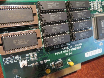
A combination of factors were required for 1280x1024x256c to be realised: faster MCLK, faster FPM DRAM, faster RAMDAC, and a modified VGA BIOS.
A 65 MHz MCLK is required for 1280x1024x256c at 60 Hz.
At the FIFO threshold included in your BIOS. This threshold is adjustable. Programming the card to use earlier FIFO refills will allow lower memory clocks, possibly at severe cost of drawing performance, though. As I undestand the ARK chip from reading the X-Server source, the display FIFO on that chip is 8 "words" of 32 bits (4 pixels at 256c), and the BIOS requests a refill threshold of "start refilling when 4 words are free", so refill is requested at 16 pixels still in the FIFO. This threshold is equal for 87i and 60p. You might be able to go back to 55MHz memory clock if you patch 47FF from 0C to something lower (but still 8 or higher). The Linux X Server XFree86 uses 0C as "standard configuration", and uses 0A if you set the option "fifo_conservative". Using 0A at 47FF will be a good start. (of course, you also need to increase another byte by 2 if you decrease this byte by 2).
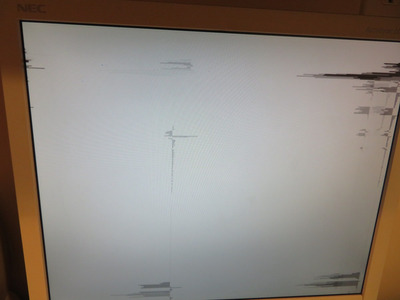
feipoa wrote on 2023-10-03, 10:48:
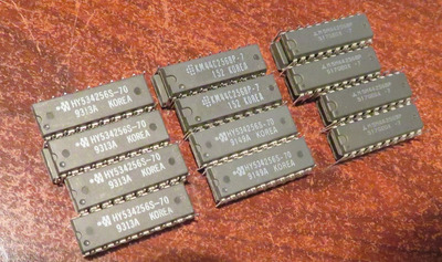
70 MHz was too fast for my 70 ns Fast Page DRAM modules; there was immediate corruption in the display right at system power-on. Even at 65 MHz with 70 ns DRAM, if left running for a few minutes, I started to see some red pixels appear when moving the Display Properties box around in circles.
This seems to indicate that reading still worked at 65MHz, but when the accellerator started high-speed writes at 65MHz, the RAM couldn't cope with it. Issues like this are typical for RAM chips that are too slow (and note how "memory chips too slow to follow MCLK" looks completely different from "MCLK to slow to satifsy video output").
feipoa wrote on 2023-10-03, 10:48:
Will there be any visible benefit in running MCLK at 70 MHz or 80 MHz, like sharper image, less shadowing, etc?
As you likely understand by now, MCLK does not directly affect the display. It affects the total available memory bandwidth. If MCLK is high enough for the given VCLK and FIFO refill threshold, the ARK1000 chip produces "pixel perfect output", increasing MCLK further doesn't change anything. So there won't be any image quality advantages by increasing MCLK. On the other hand, the speed of the accellerator scales linearly with MCLK, so the operation of copying a window when "moving it around in circles" gets faster with higher MCLK. Furthermore, higher MCLK allows more aggressive FIFO settings, increasing the band width available to the accellerator (or the VL bus) even more.
feipoa wrote on 2023-10-03, 10:48:
I then tried to run my original ARK1491 RAMDAC instead of the 110 MHz ATT RAMDAC. While it worked for the few minutes I tested it, the texted seemed blurrier and was starting to irritate my eyes.
So it seems that the chip is able to process the digital data at 110MHz correctly (you would get miscolored or flickering pixels if it does not), but the analog output stage is not up to the job for 110MHz signals. This is likely not a "manufacturing quirk", but done on purpose. If you include higher frequencies in the display output, the whole system (graphics card, monitor cable, monitor itself) will radiate more radio interference. To reduce radiated emissions and get FCC certification (or other regulatory bodies around the world), it makes a lot of sense to not create "sharper" signals than required.
feipoa wrote on 2023-10-03, 10:48:
Next I tried to use the original 2themax VGA BIOS again, with MCLK set to 65 MHz, but it insisted on interlaced mode at 1280x1024x256c.
I bet one of the 4.7k resistors on the card tells the BIOS to enable the 110MHz mode. The BIOS will read a configuration strap register whenever you try to set a video mode, and lock out the highest refresh rates on 1280x1024 if it find the "low-speed DAC" bit set. It is likely that R1, R2 and R3 are configuration straps. As R1 is connected to the 0WS jumper, this one is definitely not the 80/110 selection resistor. Usually, configuration straps have internal pull-ups (this is the native behaviour for TTL I/O pins anyway), and the external resistor is a pull-down to ground. As a "zero" in this bit means: "high speed DAC" and a "one" mean "low speed DAC", it is more likely that a "missing" resistor indicates "low speed". If the "left" pad of R2 is connected to ground, the chance is quite high that installing a 4k7 at that position will unlock the 60Hz mode even with the original bios. My BIOS patch makes the BIOS ignore this configuration strap.
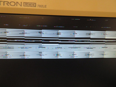
feipoa wrote on 2023-10-03, 10:48:
The resolution sheet provided in the Bali32 manual states that 800x600x16M colours is possible at 56 Hz and 60 Hz, however I could not get this mode to display. This is the result:
ARK1000VL_at_800x600xtrue_failure.jpg.JPG
Is a BIOS hack also required for this mode?
800x600x16M is also hidden behind the 110MHz lockout. As my BIOS patch disables the lockout completely, it also enables this mode. The original BIOS without strap adjustment will ignore any request to switch to this mode.
Last but not least, there also is a 1600x1200x256 interlaced mode (mode number 44h) which is also gated by the 110MHz DAC option.