VOGONS


First post, by iyatemu

User metadata
Rank Newbie
Rank
Newbie

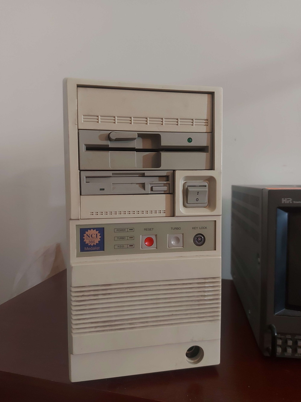
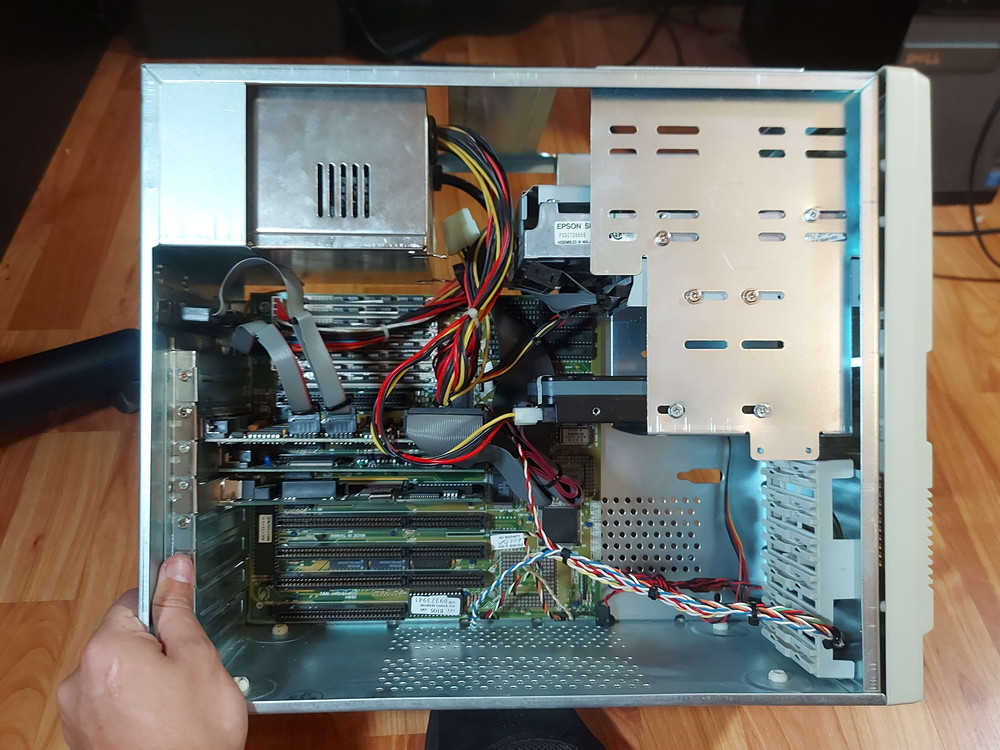
This is Camelia. She's a 386 PC I bought on ebay a few weeks back. The entire system seems to have initially been put together by an OEM called NCI. Every part inside had "NCI" warranty stickers and that badge in front seems to have a model name too (NCI Medalist 386).
Everything has a sticker. 4 of the 8 RAM sticks, the 3.5", the 5.25", the motherboard, the PSU, the interface card, and even the VGA card. The only things that weren't original are, again 4 of the 8 RAM sticks, a Linksys Ether16 card in the 4th slot, and a Caviar 2700 with a pretty barebones DOS 6.22 install on it (at the time)

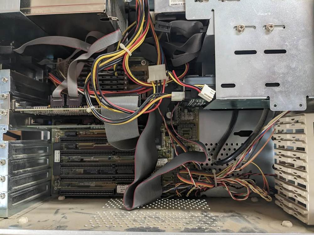
This is my first foray into retro x86 systems coming from MSX, so this whole world is new to me, so of course the machine I go for just happens to be ripe for potential upgrades and overclocking assuming everything goes right. First step was to strip her down, clean her up and get her put back together (the floppy drives were extra fun to get inside of).

9aihk6.jpg

As soon as I got it out of the box:
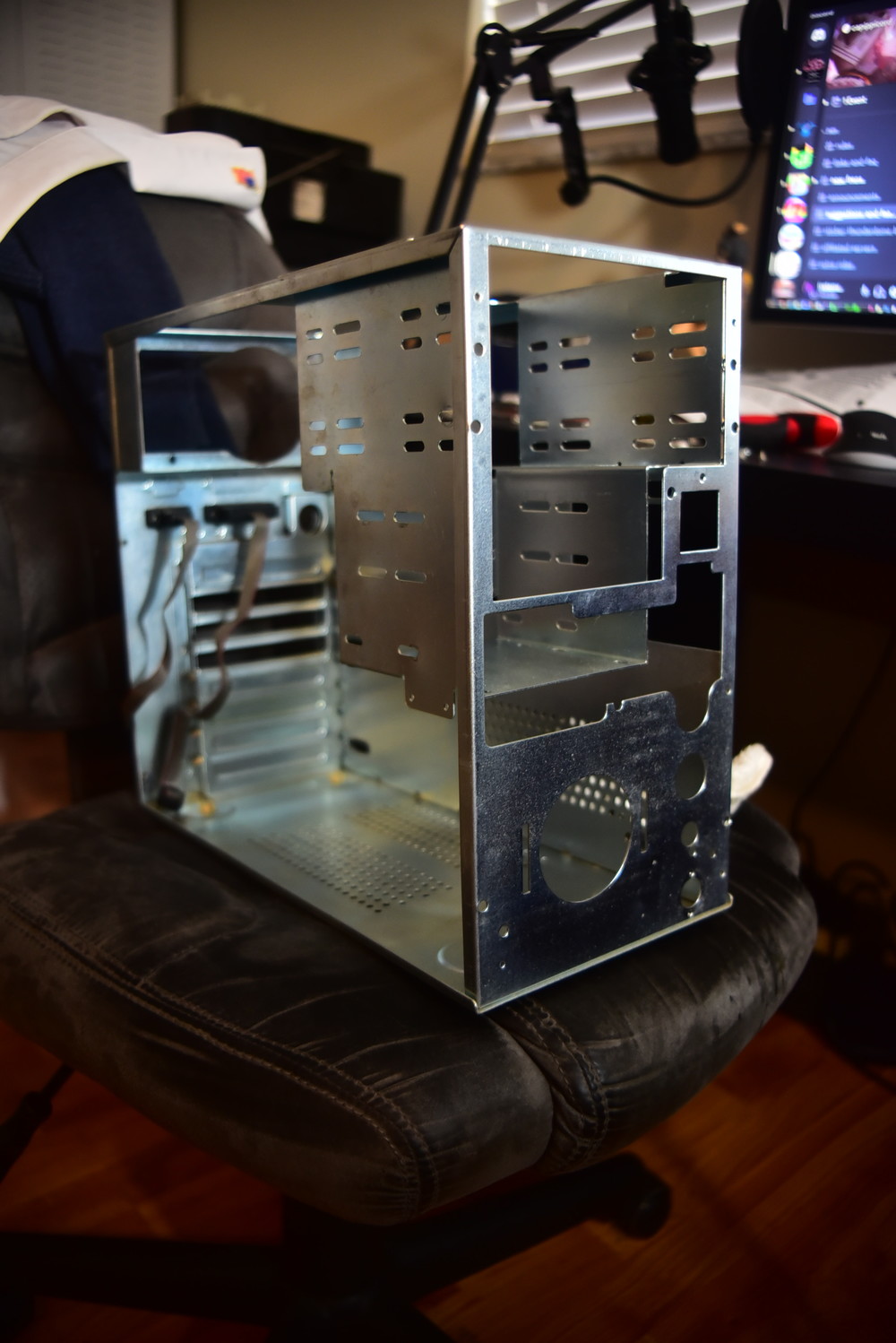
yg78ib.png

Stripped down:
tyugln.jpg

Fully cleaned:
xnomy7.jpg

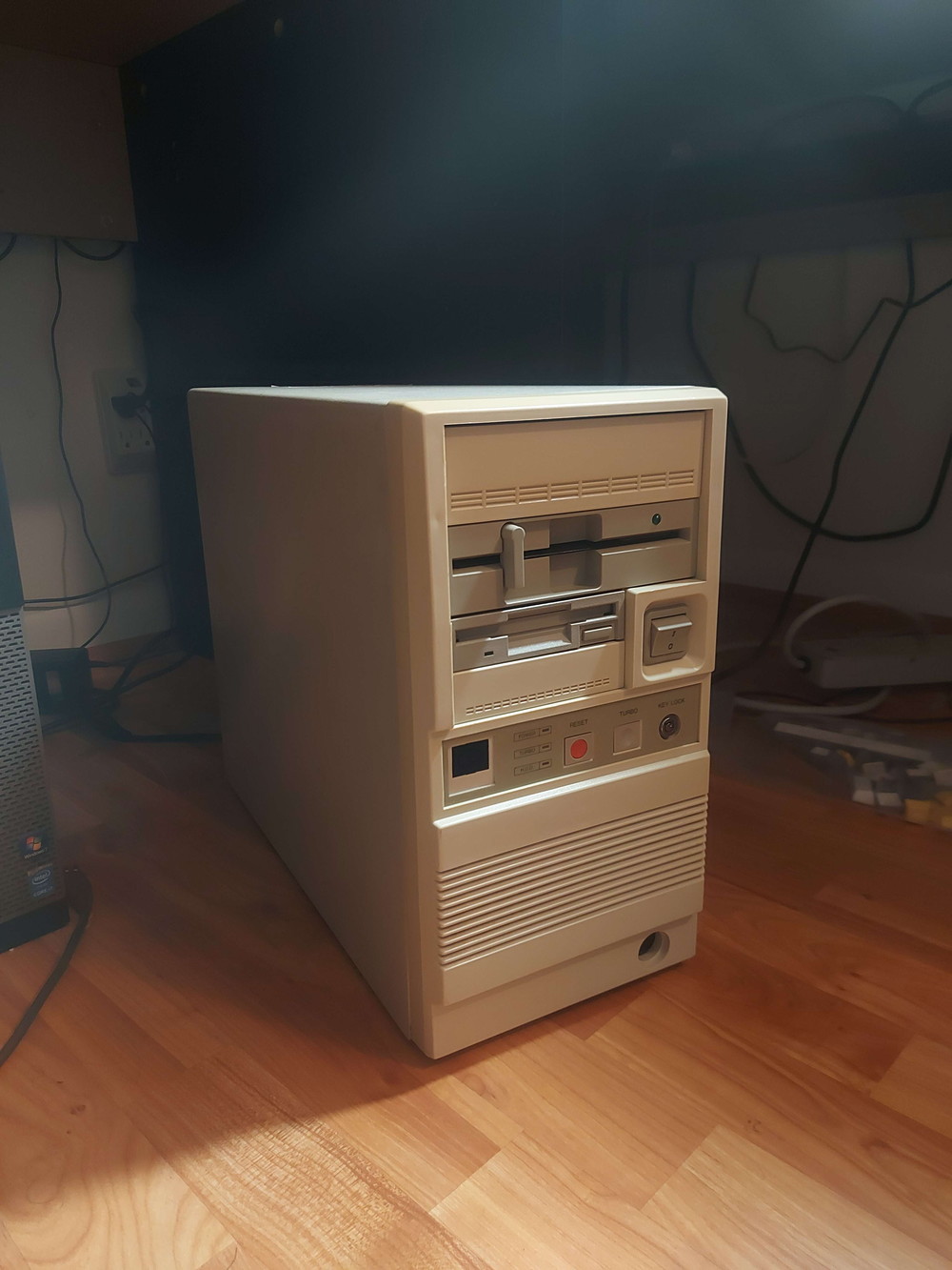
Reassembled (I drilled out and retapped the case screw holes, all of them were empty but one):
snwzmz.jpg

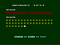
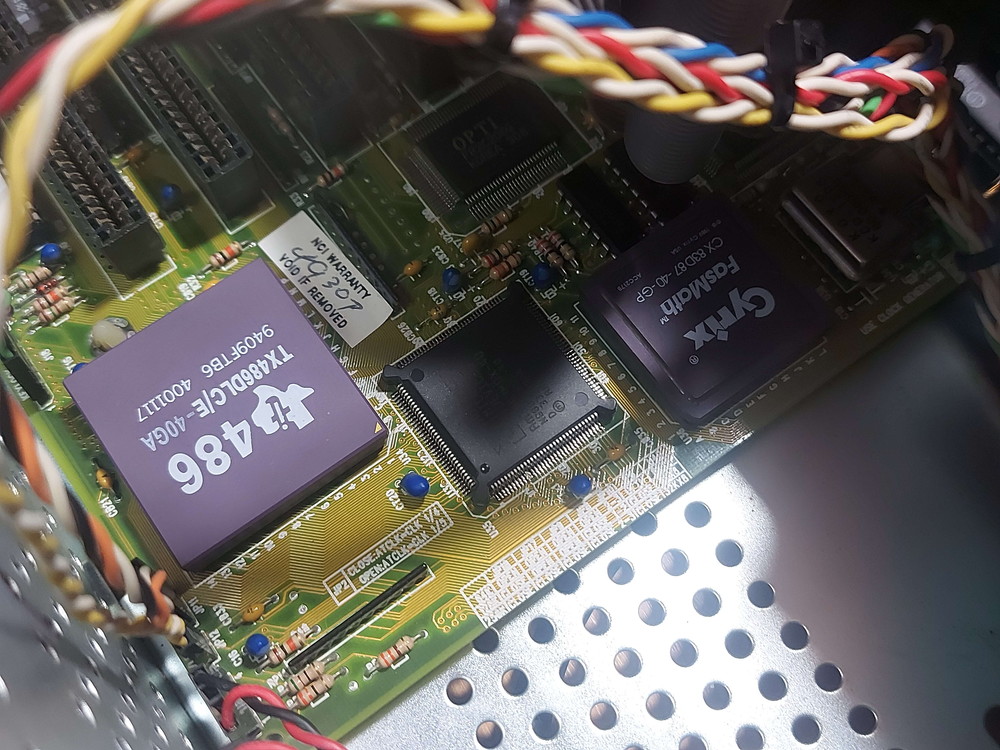
After a few days of troubleshooting and testing everything (since trying to dump the BIOS corrupted it and bricked the machine temporarily), I was finally confident enough in stability to put a Tx486DLC/E-40 and 40 MHz FasMath (black top) in.
rwe821.jpg

With that little bit of backstory over, with a couple of little details sprinkled in, we can begin.

As you can imagine, this doesn't work immediately. This is where the fun starts.

This is my motherboard: https://theretroweb.com/motherboards/s/digicom-386h
https://stason.org/TULARC/pc/motherboards/U/U … D-486-386H.html
Seriously. Actually. The pictures are of my actual personal PCB.

The relevant place to look first is obviously the section labeled "CPU TYPE CONFIGURATION". This is where my problems are stemming from.
There seems to be very little documentation about this PCB and its other variants with different jumper positions/placements. Mine (the 386H) has virtually none. Until mine was submitted the chipset wasn't known, the manufacturer wasn't known, there was no BIOS dump (in a way there still isn't since mine was corrupted), and only the stason and RetroWeb jumper settings to go off of (we'll get to that).
Here are other boards that are nearly identical with some very important (imo) differences.

Taiwan Turbo Tec 386DX Cache
https://theretroweb.com/motherboards/s/taiwan … tec-386dx-cache
JUKO 386DX Writeback:
https://theretroweb.com/motherboards/s/juko-386dx-w-b
This one is the most interesting to me:
Magitronics A-B345G and -H
https://theretroweb.com/motherboards/s/magitr … a-b345g-a-b345h
(it has the full clock multiplier/selection circuit)

As you can see, none of them have the 3-pin J20 jumper, the documents for a few of them state that the location for jumper J1 is undocumented or unknown despite being in the silk screen markings (right next to the DLC socket and under the DX), and all of them having a J13 that's not present on my board.
That there was the first hurdle. The addition of jumper J13. Initial testing of the PCB revealed that DLC B12 (KEN#) is directly connected to AmDX 54 (FLT#). Initially not knowing how this pin worked I assumed that it was tied to the GND next to it and it was serving dual-purpose as both cache-enable and 386-disable. I was wrong about it, and it was a simple enough add. J13 ties KEN# and FLT# to GND.
y96pqz.jpg

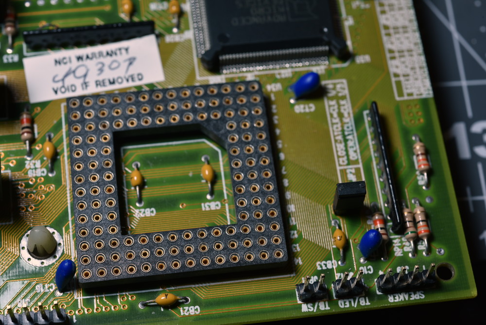
Note again that J13 and J1 are completely absent on the silk screen for my PCB. Cyrix support seems to be completely undocumented on the PCB itself.
After connecting the unlabeled J13 and attempting to boot the machine in its unique "documented" Cyrix configuration, where J5 (present on all variants) and J20 (present only on mine) are connected, I was met with a HIMEM error and told that the A20 gate could not be controlled.

This is extremely similar to the issues faced by Feipoa here.
However, none of the HIMEM switches here seem to work. I've also tried the other "compatible" /M: settings; 1, 11, 12, and 13. The machine loads HIMEM and then stops at [HIMEM is testing extended memory..._]

I'm stuck here. The PCB boots fine with the DLC in place, J5 closed, but J20 completely open. It doesn't seem as though the internal cache is working though, as no tests bring it up. The Cyrix tool (from Cyrix themselves, the blue-screen one) SAYS that the internal cache enable bit is set, but on its A20 screen says that Motherboard A20 is unmasked, Keyboard A20 is unmasked, and Fast A20 Gate is undetected despite being enabled in the BIOS (which I replaced). Internal Cache is also enabled in the BIOS (which I assume is setting the bit in the Config register).

BACK TO THE OTHER VARIANTS.
J1 is not undocumented. ALL variants of this board have its solder locations present. J1 connects the keyboard controller D1 pin to a pulldown resistor. What this does, I have no idea. Perhaps that 's why it was omitted from the Magitronics and Juko (which is populated with an SXL2-50 in one picture. J1 is obviously not necessary for Cyrix use.)
My board seems to function with J20 open, though I can't seem to get the cace to pop up. Turns out J20 might be so called because it's actually an A20 jumper. The middle pin goes to the DLC's A20M# pin. the other two pins connect A20M# to [1,2] ISA bus A20 through a 74F254 transceiver, or [2,3] DIRECTLY to the keyboard controller P21 output which seems to output the state of A20.

I have only tried running the PC with J20 set to (1,2) as the documentation states or completely open, which allows the PC to boot and HIMEM to start. It should be noted that no connection is made to the Am386DX, the state of J20 does not affect it at all. in fact it arrived to me with pins 1 and 2 connected. It's unlikely the previous owner did this and it was set from the factory.

The only possible outcomes in my mind are:
1. my board is very early and does not correctly support Cyrix chips, which is why it's totally unmarked
2. my board is very early and does not support Cyrix chips, so it was revised and the revisions are wrong still wrong (until you get to the JUKO which removes the requirement for JP1)
3. the documentation for J20 is "conceptually" backwards (it shouldn't be connected at all) and my board is somehow later (despite being 6 weeks older than the Magitronics according to the date stamps in the copper) and intentionally does not support Cyrix which is why the silk screen and JP13 (Am386 disable) was removed.
4. the documentation for J20 is electrically backwards and it should be pins [2,3] (KB A20) connected instead of pins [1,2] (74F245/ISA A20) (I have not attempted this)
5. The 74F245 is bad.
6. I've not enabled KEN# in the CPU config (its state is apparently ignored after reset and needs to be re-enabled manually. I have no idea how to do that automatically if this is the issue.)
7. The BIOS I replaced my corrupt BIOS with is missing features for 486DLC CPUs (this is the most unlikely scenario since it's pulled from another one of the other variants).

Should I keep trying? Should I give it up? Is it even possible to run Cyrix with cache on boards like this one if anyone else has a similar one? I suppose my one consolation is that even without cache a DLC40 is way faster than a DX40, and the interposer in this thread. would theoretically make an 80 MHz 386 machine possible (even without cache). I suppose another upside is that even if the project is toast I still have a complete setup and very attractive case (in my opinion) that I can put another motherboard in.

Thanks to any answers in advance.

Reply 1 of 20, by jmarsh

User metadata
Rank Oldbie
Rank
Oldbie

I think A20M# should be connected to the keyboard controller (A20 gate). It's so the CPU's internal cache knows whether or not to pay attention to the A20 address line. It doesn't affect the 386 because that has no internal cache.

Reply 2 of 20, by aitotat

User metadata
Rank Member
Rank
Member

When my 486DLC-40 broke I got A20 errors. It was on a motherboard where the DLC had previously worked. For a long time I though the problem was with motherboard but no, eventually I found out that L1 cache inside the DLC broke but the CPU works with L1 disabled.

Reply 3 of 20, by iyatemu

User metadata
Rank Newbie
Rank
Newbie
jmarsh wrote on 2023-07-18, 04:25:

I think A20M# should be connected to the keyboard controller (A20 gate).

I've just put everything together and booted with the jumper set to 2,3 (and all of the HIMEM switches removed). The system boots just like if the jumper were left open. No HIMEM error, but the Cyrix tool reports the A20 lines unmasked, and Fast A20 Gate as undetected. Is there any way to really test if the L1 cache is enabled? Speedsys seems to give the same results as well, where the processor scores 10.10 and the cache reported as "L1" is 128k (the full L2 cache amount).
FLSH# and A20#M are both enabled in the Cyrix configuration tool.
tl;dr: the system is behaving as though J20 is open when the jumper to the KB controller is closed

aitotat wrote on 2023-07-18, 04:52:

When my 486DLC-40 broke I got A20 errors. It was on a motherboard where the DLC had previously worked. For a long time I though the problem was with motherboard but no, eventually I found out that L1 cache inside the DLC broke but the CPU works with L1 disabled.

I sure hope this isn't the case.

EDIT: Did a bonehead thing and decided to remove the jumper and place it on [1,2] while the machine was running, it immediately hung, so it is "checking" the line.

Reply 4 of 20, by Deunan

User metadata
Rank Oldbie
Rank
Oldbie
iyatemu wrote on 2023-07-18, 03:42:

The only possible outcomes in my mind are:
1. my board is very early and does not correctly support Cyrix chips, which is why it's totally unmarked

This is most likely the case. In my experience the BIOS usually has some options for DLC chips but the mobo doesn't support that in HW. If the BIOS is lacking even that you are in a pretty bad spot.

So you already know FLT on the soldered 386 must be connected to GND to disable the chip. That it also grounds KEN is incorrect but rarely any chipset drives KEN anyway, and yes by default the DLC will ignore it. So that's not a problem.
What you need to know is this is not a 486 mobo. It can't deal with buit-in cache, and you already know 100% that KEN is broken. Cyrix figured that out by adding 4 exclusion zones to the CPU that specify which address spans are not to be cached. So the CPU does internally what chipset should be doing with KEN, and typically on a PC you have 2 exclusion zones: for VRAM and ROM extensions. By default the CPU will come out of reset with one zone that excludes all 4G of address space - so even if some sofware enables cache via CR0, it won't cache anything.

What BIOS should do is set the exclusion zones (the 2 mandatory ones on PC and maybe 2 extra that it allows to be configured via BIOS menu). Yours probably doesn't do it, or worse yet it removes the one blocking exclusion zone and enables cache while doing nothing else. This is the worst case scenario and it breaks a lot of things even during system boot.

From HW perspective at the very least you need the option to run hidden refresh in BIOS, and have a signal from chipset to CPU that reflects A20 gate. Both can be worked around with CPU settings via Cyrix tool but the performance loss will be substantial, pretty much you could just not turn on cache at all, it would be easier at least. Just replacing 386 with DLC chip will get you some 10% or so extra performance (cache disabled) but that depends on particular piece of software.
If you have hidden refresh then A20 gate signal perhaps can be routed from the chipset to the socket - I did that, you will need to find the datasheet for your particular chipset and it needs to have the pinout in it. Not all chips will have that signal on the pins, if it's one-chip solution then there's no need, so it might be missing. Another option might be, if there is a switch in BIOS to disable Fast A20 Gate, to generate this signal via keyboard controller as it was used to be done in original 286. It's not that much slower in most cases but a) it needs to be there in BIOS and b) the KBC must actually produce that signal. Then you can run a wire from KBC to CPU socket and fix the issue. As to what pin that signal would on KBC... well, that's a mystery. It's often pin 22 but not always, but that perhaps can be figured out with some custom software that toggles A20 gate and a volt meter - one pin on the KBC will be changing the logic level.

All in all, it can be done, I've modded some mobos, but the difficulty level can vary and usually some soldering is required.

Reply 5 of 20, by iyatemu

User metadata
Rank Newbie
Rank
Newbie
Deunan wrote on 2023-07-18, 23:23:
iyatemu wrote on 2023-07-18, 03:42:

The only possible outcomes in my mind are:
1. my board is very early and does not correctly support Cyrix chips, which is why it's totally unmarked

This is most likely the case. In my experience the BIOS usually has some options for DLC chips but the mobo doesn't support that in HW. If the BIOS is lacking even that you are in a pretty bad spot.

A lot of the stuff you've mentioned here is already either addressed in my post or an assumption on your part.
Just in case, though, I've attached pictures of the BIOS options in the BIOS I replaced my original corrupted one with (Like I said, it's from one of those similar boards I also linked to). You are correct that nothing seems to be set up in the non-cacheable areas. I have no idea what to set them to, but it IS present unlike what you seem to have assumed. That might actually be the entire issue.
jADreXw.jpeg
ub5E6az.jpeg

For example, running a line from the KB controller to the CPU A20M# pin is something I've already done. J20 does this when set to [2,3]. In fact, doing what you said here...

Deunan wrote on 2023-07-18, 23:23:

Another option might be, if there is a switch in BIOS to disable Fast A20 Gate, to generate this signal via keyboard controller as it was used to be done in original 286. It's not that much slower in most cases but a) it needs to be there in BIOS and b) the KBC must actually produce that signal. Then you can run a wire from KBC to CPU socket and fix the issue.

...actually RETURNS the A20 HIMEM errors. So this either means that the KBC is NOT generating A20 on Pin 22, or something else since Fast Gate A20 needs to be on for the PC to boot at all.

In the current configuration, the BIOS option for A20 Fast Gate is on, AND the KBC is connected to the CPU. I've tried 5 combinations for J20 and Fast Gate.
1. J20 [1,2] (ISA A20) + Fast Gate ON - HIMEM errors
2. J20 [2,3] (KBC A20) + Fast Gate ON - boots into DOS with HIMEM << current setup
3. J20 [OPEN] + Fast Gate ON- Boots into DOS with HIMEM
4. J20 [1,2] (ISA A20) + Fast Gate OFF - HIMEM errors
5. J20 [2,3] (KBC A20) + Fast Gate OFF - HIMEM errors

Also, for what it's worth, it seems like the cache *DOES* actually seem to be working to an extent, unless the Cyrix test software is lying (it's for a 486SXL/C, posted here).
McZXXUQ.jpeg
9qi8qWq.jpeg
zD2A0l9.jpeg
kVeqD0E.jpeg

My question is, if it is working, is it actually usable? if it IS real, then the board obviously support it natively, and the J20 jumper documentation is wrong. I'm guessing the issue now is that the non-cacheable areas aren't set in the BIOS. What should the non-cacheable areas be set to? Or am I completely wrong? Remember the system works opposite to how you say it should. Fast Gate is enabled, but the CPU is connected to the KBC and cache seems to be functioning, at least with Cyrix's own test/config software. This entire situation is very confusing, but that specifically seems very off to me.

Reply 6 of 20, by kixs

User metadata
Rank l33t
Rank
l33t

Your motherboard is from 1992. So not an early model. If it doesn't have option for L1 cache, you can always enable it via software. Otherwise DLC is drop in replacement and should work out of the box - usually no need to change any jumpers.

Your last post and BIOS screenshots show Internal cache is enabled. So it should work with L1 cache enabled - check with benchmarks.

Requests are also possible... /msg kixs

Reply 7 of 20, by Deunan

User metadata
Rank Oldbie
Rank
Oldbie
iyatemu wrote on 2023-07-19, 03:41:

My question is, if it is working, is it actually usable?

It sure is, usually if the A20 gate signal is not passed to the CPU you will get system hangs when you attempt to load DOS high after HIMEM. Now I prefer to use command-line Cyrix tools to query/set the various features but that software you have shows some nice advanced features like testing and easy A20 status test.

What the "Fast A20 Gate" option does, actually, is always a mystery. The idea is to do the masking in-chip because that's way faster than addressing KBC over the slow ISA bus protocol. So it would make most sense that, when enabled, the chipset intercepts all such I/O attempts and never even bothers to tell the KBC because that costst time, and we are specifically trying to avoid that penalty. So with that BIOS option on the KBC usually doesn't drive the line properly, thus in neeeds to be disabled.
On the other hand many such mobos don't do anything with KBC generated A20M signal, so it has to be enabled to fast mode or it will simply not work at all. And here's the problem with DLC chip - you can have the signal working but the CPU doesn't know its state, or you can make the state know but prevent it from actually doing anything.

So it would seem your particular mobo does the A20 masking in the chipset only using the internal settings so it needs the fast setting. But fortunately the I/O is being passed to KBC anyway so it can then generate the required signal for the CPU - so it's not really "Fast", but "Internal" in your case. Different mobos might do things differently - I have some experience with that.

Anyway, your BIOS has the required options for exclusion zones so it sets the CPU properly after reset, which is nice because using the software tool to do that has some limitations (it would mostly be Win 3 related). The tool you have shows A20 mask being passed to CPU and all other tests pass, I think you are good to go. No need to tweak anything. Just write down what the jumpers need to set to for future reference and keep in mind even manuals that explain those are often wrong. Also, connecting ISA A20 to A20M input on CPU is not the right way to do it, I wonder why such option even exists, perhaps whoever made that mobo didn't actually understand what the Cyrix needs and had no CPU to test. But they did provide options that work.

EDIT: Forgot to add, do make sure your DLC is set to BARB flushing (and that you keep that Hidden Refresh enabled). If the tool you have doesn't show it, try the command line one. I've seen these CPUs set to use FLUSH signal and "work" even in the absence of one, because the small cache is often trashed before it can return stale data. But these chipsets can't produce FLUSH so BARB must be used instead.
Also, these BIOS timings are way too conservative. Try 1WS for RAM and 0WS for cache write, and 2-x-x-x for cache read. Of these the cache read is the most sensitive (and x means doesn't care on 386 system, but if there is a setting for 2 and 1 try 1). In each case, if the system doesn't crash right away during boot, try running Doom in demo loop - it's a very good stress test of the cache actually. If that passes try old memtest86 or GoldMemory to verify everything is stable, make sure you do a few complete passes.

Reply 8 of 20, by iyatemu

User metadata
Rank Newbie
Rank
Newbie
kixs wrote on 2023-07-19, 07:18:

Your motherboard is from 1992. So not an early model. If it doesn't have option for L1 cache, you can always enable it via software. Otherwise DLC is drop in replacement and should work out of the box - usually no need to change any jumpers.

Your last post and BIOS screenshots show Internal cache is enabled. So it should work with L1 cache enabled - check with benchmarks.

The whole reason I made this thread is the cache not being detected by typical benchmarks. If you can suggest some that might be able to detect it, sure. Otherwise I have no idea where to start.

Deunan wrote on 2023-07-19, 09:01:
iyatemu wrote on 2023-07-19, 03:41:

My question is, if it is working, is it actually usable?

It sure is, usually if the A20 gate signal is not passed to the CPU you will get system hangs when you attempt to load DOS high after HIMEM. Now I prefer to use command-line Cyrix tools to query/set the various features but that software you have shows some nice advanced features like testing and easy A20 status test.

Great.

Deunan wrote on 2023-07-19, 09:01:

your BIOS has the required options for exclusion zones so it sets the CPU properly after reset, which is nice because using the software tool to do that has some limitations (it would mostly be Win 3 related).

In the event I need to set them (like installing Win3.11 or later) What should they be set to? Is there a universal set of values or do different address ranges/MB boundaries need to be tested one by one?

Deunan wrote on 2023-07-19, 09:01:

Also, these BIOS timings are way too conservative. Try 1WS for RAM and 0WS for cache write, and 2-x-x-x for cache read. Of these the cache read is the most sensitive (and x means doesn't care on 386 system, but if there is a setting for 2 and 1 try 1). In each case, if the system doesn't crash right away during boot, try running Doom in demo loop - it's a very good stress test of the cache actually. If that passes try old memtest86 or GoldMemory to verify everything is stable, make sure you do a few complete passes.

Thanks for everything. Though now, why aren't tools like speedsys and cachechk detecting and testing it?
Are there other tests (besides the blue cyrix ones) that can detect it?
How do I automatically load register configs into the chip? Just a line in AUTOEXEC?

Last edited by iyatemu on 2023-07-19, 13:34. Edited 1 time in total.

Reply 9 of 20, by kixs

User metadata
Rank l33t
Rank
l33t

Try running any benchmark (3dbench, NSSI, Checkit, Comptest...) with and without Internal cache in BIOS enabled. You should get ~20% difference.

Comptest will detect internal cache.

Requests are also possible... /msg kixs

Reply 10 of 20, by iyatemu

User metadata
Rank Newbie
Rank
Newbie

I also went ahead and installed an SB16 I had laying around last night. Everything went well but during the self-test it complained about thd 16-bit DMA. Played all sounds fine, though. This doesn't have anything to do with the L1, does it? Just covering my bases.

kixs wrote on 2023-07-19, 13:27:

Try running any benchmark (3dbench, NSSI, Checkit, Comptest...) with and without Internal cache in BIOS enabled. You should get ~20% difference.

Comptest will detect internal cache.

I'll try these once I get home, thank you.

Reply 11 of 20, by Deunan

User metadata
Rank Oldbie
Rank
Oldbie
iyatemu wrote on 2023-07-19, 13:10:

Thanks for everything. Though now, why aren't tools like speedsys and cachechk detecting and testing it?
Are there other tests (besides the blue cyrix ones) that can detect it?
How do I automatically load register configs into the chip? Just a line in AUTOEXEC?

Most tools can't detect cache memory that small - reason being the detection code is already taking a significant amount of it by itself. It's not impossible if the code is small and crafed properly, but I guess it rarely is, most of it was designed to work with 8k of Intel 486 and above. It doesn't help that SLC/DLC chips cache and track 32-bit words rather than 16-byte lines and the cache is at best 2-way, or even directly mapped as an option, so it trashes easily. 1k of L1 doesn't make a dent in CACHECHK results for example.

The best way to tell is to compare benchmark results with L1 on and off. Some programs might seem like they detect the cache but actually cheat a little - like NSSI. It just assumes that if DLC chip is detected then L1 is 1k in size. I don't think it actually tests the size - I could be wrong but I've seen it glitch SXL chip once and report wrong values. You can also use the command line Cyrix tool to tell what settings the CPU is running with as well.

Yes, the AUTOEXEC route is the best, if your mobo boots that far with what BIOS set the DLC to, since some device drivers might get confused if the cache is enabled too early. For your mobo I would use these settings:
* FLUSH and KEN off, BARB enabled (BARB is not an input, as such, more like a method that uses HOLD to detect DMA cycles)
* A20M input enabled, workaround (non-cacheable first 64k of each 1M segment) disabled
* L1 enabled in CR0, obviously
* exclusion zones: 0xA000 - 128k (for VGA VRAM in both text and graphics modes) and 0xC000 - 256k (for any other cards with their own memory or possibly banked ROMs) - of these the VRAM is the more important usually

Sometimes the 0xC000 zone can be skipped if there are no advanced ISA cards in the system, that will provide a small performance uplift for code/data loaded into UMB areas. But it's not worth the trouble of having to remember about it every time you want to install a SCSI card or something of the sort in my opinion.

Reply 12 of 20, by iyatemu

User metadata
Rank Newbie
Rank
Newbie
Deunan wrote on 2023-07-19, 14:02:
For your mobo I would use these settings: * FLUSH and KEN off, BARB enabled (BARB is not an input, as such, more like a method t […]
Show full quote

For your mobo I would use these settings:
* FLUSH and KEN off, BARB enabled (BARB is not an input, as such, more like a method that uses HOLD to detect DMA cycles)
* A20M input enabled, workaround (non-cacheable first 64k of each 1M segment) disabled
* L1 enabled in CR0, obviously
* exclusion zones: 0xA000 - 128k... and 0xC000 - 256k...

Fortunately from what I saw last night, most of this seems to be already set correctly, only difference is switching FLUSH for BARB. Amazing that this mobo seems to have "just worked" with the DLC and I just had no idea what I was doing or what to look for.

Reply 13 of 20, by kixs

User metadata
Rank l33t
Rank
l33t

486DLC is a drop in replacement for 386DX. Worst case you need to enable L1 via software. There could be some compatibility issues with early boards.

Requests are also possible... /msg kixs

Reply 14 of 20, by iyatemu

User metadata
Rank Newbie
Rank
Newbie
Deunan wrote on 2023-07-19, 14:02:
Yes, the AUTOEXEC route is the best, if your mobo boots that far with what BIOS set the DLC to, since some device drivers might […]
Show full quote

Yes, the AUTOEXEC route is the best, if your mobo boots that far with what BIOS set the DLC to, since some device drivers might get confused if the cache is enabled too early. For your mobo I would use these settings:
* FLUSH and KEN off, BARB enabled (BARB is not an input, as such, more like a method that uses HOLD to detect DMA cycles)
* A20M input enabled, workaround (non-cacheable first 64k of each 1M segment) disabled
* L1 enabled in CR0, obviously
* exclusion zones: 0xA000 - 128k (for VGA VRAM in both text and graphics modes) and 0xC000 - 256k (for any other cards with their own memory or possibly banked ROMs) - of these the VRAM is the more important usually

Sometimes the 0xC000 zone can be skipped if there are no advanced ISA cards in the system, that will provide a small performance uplift for code/data loaded into UMB areas. But it's not worth the trouble of having to remember about it every time you want to install a SCSI card or something of the sort in my opinion.

Been playing with the switches and I didn't notice any change between FLUSH# and BARB, though I'm not sure it's something I'd be able to notice. Speedsys results changed with cache enabled vs disabled, though, so it is definitely accessible and being used. The board/CPU seems to load the optimal settings by default, even enabling the correct non-cacheable areas. The only thing that may be different is FLUSH# vs. BARB, but again, everything so far seems to have functioned well without switching inputs.

I'll do more thorough, actual testing tomorrow, but for now I just need to figure out a file transfer solution that's more efficient than transferring files over 720k at a time with an MSX2 as an SD - Floppy translator.

Reply 15 of 20, by Deunan

User metadata
Rank Oldbie
Rank
Oldbie

Well, you could test if the FLUSH pin on the DLC CPU socket (E13) is connected to the chipset. I've never seen that on OPTi based mobos but then again I've never seen a proper datasheet for this chipset either. If it's unconnected and floating you are just lucky the internal leakage of the input weakly drives it high instead of low - which would put the CPU in constant cache flush mode, this inflicts some serious performance degradation.

Because of the very small L1 the un-flushed cache might appear to work correctly but sooner or later you might get silently corrutped data from floppy drives, not worth the risk. With hidden refresh BARB will work equally well except it will trigger on both DMA writes and reads. Which will have some performance impact in games using SoundBlaster for digitized audio playback. Especially in games where such engine runs all the time with software channel mixing (say, Doom for example). In these cases FLUSH would (if done properly by the chipset) not trigger and not clear all internal cache.

Reply 16 of 20, by iyatemu

User metadata
Rank Newbie
Rank
Newbie
Deunan wrote on 2023-07-20, 09:41:

Well, you could test if the FLUSH pin on the DLC CPU socket (E13) is connected to the chipset. I've never seen that on OPTi based mobos but then again I've never seen a proper datasheet for this chipset either. If it's unconnected and floating you are just lucky the internal leakage of the input weakly drives it high instead of low - which would put the CPU in constant cache flush mode, this inflicts some serious performance degradation.

Because of the very small L1 the un-flushed cache might appear to work correctly but sooner or later you might get silently corrutped data from floppy drives, not worth the risk. With hidden refresh BARB will work equally well except it will trigger on both DMA writes and reads. Which will have some performance impact in games using SoundBlaster for digitized audio playback. Especially in games where such engine runs all the time with software channel mixing (say, Doom for example). In these cases FLUSH would (if done properly by the chipset) not trigger and not clear all internal cache.

Well, bad news and good news.
Bad news: FLUSH# is not connected to any pins on the chipset.

Good news: FLUSH# IS CONNECTED VIA JP5. JP5 connects FLUSH# to a 74F00. It seems that this board generates a FLUSH# signal externally using the Serial L2 method laid out in one of the threads I linked up there earlier.

Y1 of the 7400 is directly connected to FLUSH# via JP5. The NAND inputs are:
B1 - Pin 1 of the 82C392, pin 154(?) of the 495, and pin 76 of the 206. The 206 is the only one that has a datasheet you can find. This is the HLDA signal.
A1 - 74F04 5Y, which is inverting B3 from a 74F245, 245 A3 is connected to ISA MEMW#.

So it LOOKS LIKE I don't actually need to change ANYTHING, and this board came from the factory natively fully supporting DLC chips, but for some reason had that capability disabled (no JP13, FLT#), undocumented (no silk screen), and described incorrectly (set JP20 [1,2] instead of [2,3]). I really wonder why, especially when they went through the trouble and component cost of getting FLUSH# to work too.

Thank you for pointing me in the right direction with this even though it looks like the board functioned perfectly from the very beginning. Sorry for wasting your time if I did.

Reply 17 of 20, by Deunan

User metadata
Rank Oldbie
Rank
Oldbie
iyatemu wrote on 2023-07-20, 17:51:

So it LOOKS LIKE I don't actually need to change ANYTHING

Yup, this is a HW circuit that generates the FLUSH signal on mobos that always HOLD the CPU on any DMA. Which AFAIK this OPTi chipset does. I hope I didn't send you on a merry chase for problems you don't have, but better to be sure then to discover corrupted data or suffer random system crashes.

Reply 18 of 20, by iyatemu

User metadata
Rank Newbie
Rank
Newbie
Deunan wrote on 2023-07-20, 18:59:

I hope I didn't send you on a merry chase for problems you don't have, but better to be sure then to discover corrupted data or suffer random system crashes.

Not at all. I tried tracing JP5 when I first got the board but got lost because I started from the jumper itself which was in the middle of the path. It was very informative and now makes me even more curious about the other boards.

This one looks like it can be permanently set up for DLC use. Maybe that's why it wasn't silk-screened. The back of JP5 has a solder pad jumper unlike any of the other ones. I still have no clue what the purpose of JP1 is (pulldown on KBC Data 1). Some of the other boards have that marked as being Closed for Cyrix.

I have to be on the look out for more of these mobos now. Next step is to try overclocking this thing.

Reply 19 of 20, by Deunan

User metadata
Rank Oldbie
Rank
Oldbie
iyatemu wrote on 2023-07-20, 23:26:

I have to be on the look out for more of these mobos now. Next step is to try overclocking this thing.

Just FYI the DLC chips don't really overclock, not from 40MHz upwards, and since the mobo pretty much runs at CPU bus frequency it will be a limiting factor as well. Usually stable 40MHz is as good as it gets.
Also, if you were considering SXL replacement for the DLC, that usually also brings next to nothing. It might work tad bit better with FLUSH than BARB but the primary problem of these CPUs remain: the 386 bus protocol can't do burst cache line loads, so you only get speedups from code loops and frequently used data that is small enough not to spill. Which, even at 8k L1 (still 2-way at best), is difficult to achieve.