VOGONS


First post, by yjfy

User metadata
Rank Oldbie
Rank
Oldbie

Feast of the first generation GPU
yjfy​
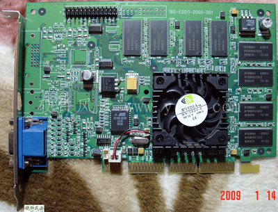
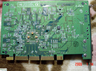
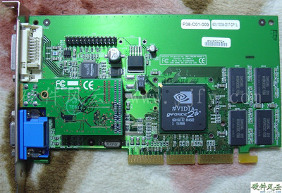
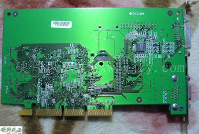
nVIDIA First to Integrate Hardware T & L (Transform and Lighting)into Geforce 256 Graphics Core,Geforce 256 was marketed as “The world's first GPU”, or “Graphics Processing Unit".Announced on August 31, 1999 and released on October 11, 1999.This is the original origin of the GPU name, but now the Graphics chip is collectively called GPU.

In fact, Geforce 256 won the title of "The world's first GPU" is very difficult, because there are two opponents in front of it.

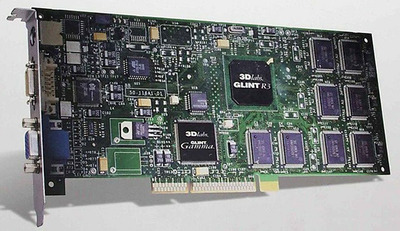
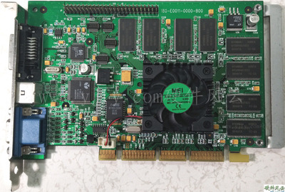
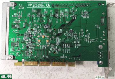
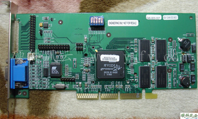
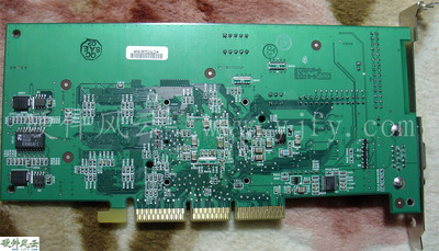
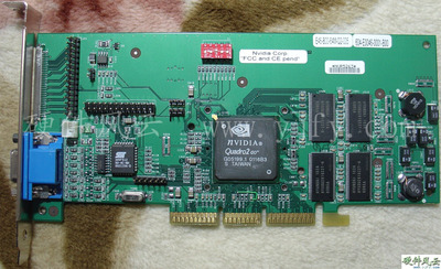
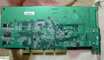
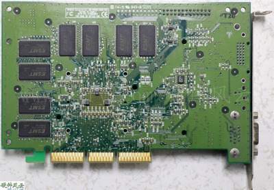
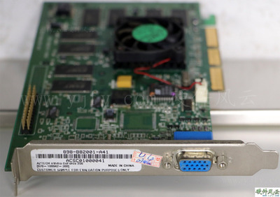
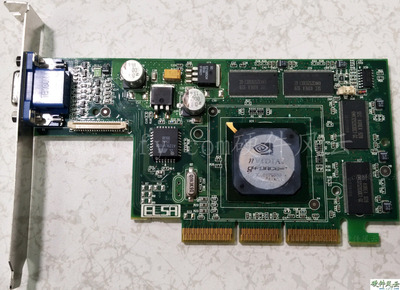
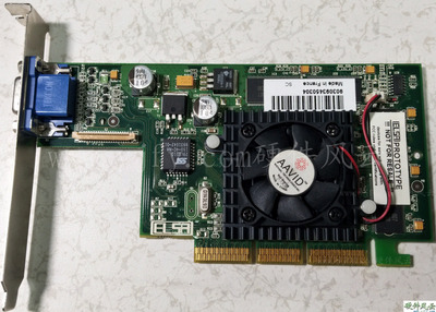
May 11, 1999 ,3Dlabs announced the Oxygen GVX1, workstation graphics card.The GVX1 does not take nVIDIA's more cost-effective route of integrating hardware T&L support into the core.this using GLINT R3(Permedia 3) and one external chip ,this chip is GLINT Gamma G1, Geometry Processor.The GLINT Gamma G1 is capable of processing 4.75 million triangles per second,Geforce 256 is capable of up to 15 million triangles per second.

Although Oxygen GVX1 is a hardware T & L graphics card before Geforce 256, but they were not integrated into the graphics core.

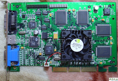
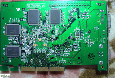
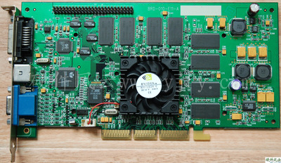
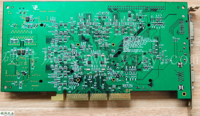
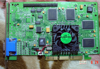
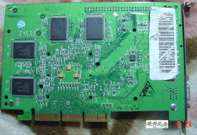
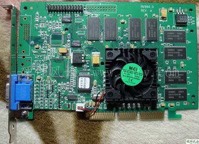
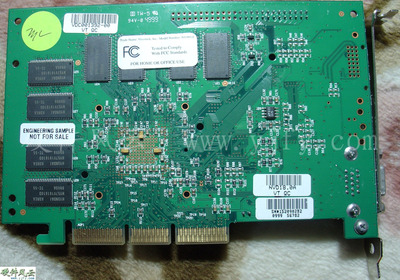
Oxygen GVX1 Engineering sample

Attachments

  • Oxygen_GVX1.jpg
    Filename
    Oxygen_GVX1.jpg
    File size
    119.64 KiB
    Views
    957 views
    File license
    Public domain

Reply 1 of 47, by yjfy

User metadata
Rank Oldbie
Rank
Oldbie

Even more shocking to nVIDIA is that the Announced date of S3's Savage 2000 was one day earlier than Geforce 256. August 30, 1999.

Savage 2000 supported S3's S3TC texture compression, a hardware transform and lighting engine named "S3TL", and was equipped with a "QuadTexture Engine" capable of a single quad-textured pixel per clock or 2 dual-textured pixels per clock.S3TL is similar to T & L. However, S3TL shipped completely non-functional, primarily because initial drivers were Direct3D 6-based (Direct3D 7 was the first release with HW T & L support).Therefore, it is not a real GPU.

Savage 2000 (GX4) Evaluation board

(From pcgameshardware de)​

Attachments

Reply 2 of 47, by yjfy

User metadata
Rank Oldbie
Rank
Oldbie

Since IBM launched the PC in 1981, more than a hundred display chip manufacturers have appeared. In the 3D graphics divide of 1995, only dozens of companies were able to bridge it. The GPU divide created by nVIDIA in 1999. Only ATi、Trident、SiS、MATROX and S3 can cross. This article focuses on nVIDIA's first-generation GPU chip graphics cards and other manufacturers' first-generation GPU graphics cards.
1. nVIDIA
1.1 nVIDIA original factory
1.1.1 Geforce 256
The announcement date of Geforce 256 is August 31, 1999 (9936 weeks), and the release date is October 11, 1999 (9942 weeks).

Technical details:
Fabrication Process: 220 nm
Reenderpiplines: 4 Pixel/4 TMU/4 ROP
Base Clock: 120 MHz
Memory Clock: 166 MHz SDR/150 MHz DDR
Memory Size: 32 /64MB
Memory Bus Width: 128-bit
Interface: AGP 4x
Pixel Fillrate (MPixel/s):480
Texel Fillrate (MTexel/s):480
Triangle/Vertices Rate (M/s):15

The date on the PCB of this Geforce 256 Reference board is 9934 weeks, which is equivalent to the beginning of September. Both are earlier than the announcement and release date.
Geforce 256 Reference board

Attachments

  • geforce_256.jpg
    Filename
    geforce_256.jpg
    File size
    982.92 KiB
    Views
    949 views
    File license
    Public domain
  • geforce_256_1.jpg
    Filename
    geforce_256_1.jpg
    File size
    803.81 KiB
    Views
    949 views
    File license
    Public domain

Reply 3 of 47, by yjfy

User metadata
Rank Oldbie
Rank
Oldbie

1.1.2 Geforce 256 DDR
Geforce 256 DDR was released on February 11, 2000 (0007 weeks). The date on this Geforce 256 DDR Reference board PCB is 9948 weeks, earlier than the announcement date in early December 1999 (9949 weeks).
Geforce 256 DDR Reference board

Attachments

Reply 4 of 47, by yjfy

User metadata
Rank Oldbie
Rank
Oldbie

1.1.3 Quadro
Nov. 1, 1999 (9945 weeks) nVIDIA Corporation today announced the Quadro workstation GPU, the newest member of the company's performance-leading family of award-winning graphics processors.

The core clock of the Quadro is 135MHz, a 15MHz increase from the 120MHz core clock of the Geforce. The higher core clock allows the Quadro to achieve a 13% higher fill rate of 540 Mpixels/s.

The PCB date of this Quadro 256 Evaluation board is 9946 weeks, one week later than the announced date.

Quadro 256 Evaluation board

Attachments

  • Quadro_ES.jpg
    Filename
    Quadro_ES.jpg
    File size
    907.37 KiB
    Views
    945 views
    File license
    Public domain
  • Quadro_ES_1.jpg
    Filename
    Quadro_ES_1.jpg
    File size
    664.43 KiB
    Views
    945 views
    File license
    Public domain

Reply 5 of 47, by yjfy

User metadata
Rank Oldbie
Rank
Oldbie

1.1.4 Quadro AGP Pro
The PCB date of the B00 version of the Quadro 256 AGP Pro Evaluation board is 9946 weeks, which is one week later than the announced date.
Quadro 256 AGP Pro Evaluation board

Attachments

Last edited by yjfy on 2020-05-09, 01:33. Edited 1 time in total.

Reply 6 of 47, by yjfy

User metadata
Rank Oldbie
Rank
Oldbie

The PCB date of the B01 version of the Quadro 256 AGP Pro Evaluation board is 9948 weeks, which is not much different from the B00 version.
Quadro 256 AGP Pro Evaluation board

Attachments

Reply 7 of 47, by yjfy

User metadata
Rank Oldbie
Rank
Oldbie

1.1.5 Geforce2 Go
On November 11, 2000 (week 0047), nVIDIA released the world's first mobile GPU Geforce2 Go at COMDEX / Fall 2000. Geforce2 Go is based on Geforce2 MX core.The following Geforce2 Go Evaluation board has a chip date of 0045 weeks earlier than the release date of 0047 weeks. The PCB date is 0050 weeks.
Geforce2 Go Evaluation board

Attachments

Reply 8 of 47, by yjfy

User metadata
Rank Oldbie
Rank
Oldbie

The following Geforce2 Go Reference board chip date is 0045 weeks and PCB date is 0033 weeks, using the Geforce2 MX Reference board type.
Geforce2 Go Reference board

Attachments

  • GEFORCE2_GO_2.jpg
    Filename
    GEFORCE2_GO_2.jpg
    File size
    361.09 KiB
    Views
    930 views
    File license
    Public domain
  • GEFORCE2_GO_3.jpg
    Filename
    GEFORCE2_GO_3.jpg
    File size
    366.22 KiB
    Views
    930 views
    File license
    Public domain

Reply 9 of 47, by yjfy

User metadata
Rank Oldbie
Rank
Oldbie

1.1.6 Quadro2 Go
Quadro2 Go is based on the core of Quadro256, the high-frequency version of Quadro2, and is the mobile version of Quadro2, with a release date of August 14, 2001 (0133 weeks). The following Quadro2 Go Evaluation board has a chip date of 0116 weeks and a PCB date of 0124 weeks.
Quadro2 Go Evaluation board

Attachments

  • Quadro2_Go_ES.jpg
    Filename
    Quadro2_Go_ES.jpg
    File size
    461.14 KiB
    Views
    930 views
    File license
    Public domain
  • Quadro2_Go_ES_1.jpg
    Filename
    Quadro2_Go_ES_1.jpg
    File size
    420.08 KiB
    Views
    930 views
    File license
    Public domain

Reply 10 of 47, by yjfy

User metadata
Rank Oldbie
Rank
Oldbie

1.2 Creative
1.2.1 Geforce 256 (3D Blaster Annihilator)
As an important partner of nVIDIA, Creative first invested in the development of Geforce 256 graphics card. It can be seen from the following version of the 3D Blaster Annihilator graphics card is 009931. Creative obtained the reference design of Geforce 256 and designed the 009931 version before the 31st week of 1999. The production date of the PCB board is 9932 weeks, that is, the PCB board is produced in the 32nd week of 1999. This date is earlier than the date of first publication on August 31, 1999 (9936 weeks). This is because nVIDIA's engineering sample graphics cards are all manufactured by Creative. In addition, the release date of 3D Blaster Annihilator is October 25, 1999 (9944 weeks), which is earlier than nVIDIA's November 11, 1999 (9946 weeks). It is inevitable that nVIDIA will be unhappy.
3D Blaster Annihilator Engineering sample

Attachments

  • CT6940_009931.jpg
    Filename
    CT6940_009931.jpg
    File size
    724.65 KiB
    Views
    930 views
    File license
    Public domain
  • CT6940_009931_1.jpg
    Filename
    CT6940_009931_1.jpg
    File size
    740.8 KiB
    Views
    930 views
    File license
    Public domain

Reply 11 of 47, by yjfy

User metadata
Rank Oldbie
Rank
Oldbie

1.2.2 Geforce 256 DDR (3D Blaster Annihilator Pro)
3D Blaster Annihilator Pro Released 12 February 2000 (0007 weeks), just one day later than the release date of Geforce 256 DDR.

This 3D Blaster Annihilator Pro graphics card is also directly used Geforce 256 DDR reference design stereotyped 009942 version, dated 9942 weeks, earlier than the early December 1999 (9949 weeks) Geforce 256 DDR announcement period. The PCB date of this card is 9941 weeks, which is earlier than the final date of 9942 weeks.

3D Blaster Annihilator Pro Qualification sample

Attachments

  • CT6970.jpg
    Filename
    CT6970.jpg
    File size
    745.63 KiB
    Views
    930 views
    File license
    Public domain
  • CT6970_1.jpg
    Filename
    CT6970_1.jpg
    File size
    371.01 KiB
    Views
    930 views
    File license
    Public domain

Reply 12 of 47, by yjfy

User metadata
Rank Oldbie
Rank
Oldbie

1.3 VISIONTEK
VISIONTEK Geforce 256 Engineering sample directly uses nVIDIA's Geforce 256 reference design, with a PCB date of 9949 weeks and later than release date October 11, 1999 (9942 weeks).
VISIONTEK Geforce 256 Engineering sample

Attachments

  • NV994.0_ES.jpg
    Filename
    NV994.0_ES.jpg
    File size
    901.96 KiB
    Views
    929 views
    File license
    Public domain
  • NV994.0_ES_1.jpg
    Filename
    NV994.0_ES_1.jpg
    File size
    502.1 KiB
    Views
    929 views
    File license
    Public domain

Reply 13 of 47, by yjfy

User metadata
Rank Oldbie
Rank
Oldbie

1.4 AZtech
The customer sample PCB date of this AZtech Geforce 256 is 9950 weeks, which appears relatively late, and is also a reference design using Geforce 256.
AZtech Geforce 256 Customer Sample

Attachments

Reply 14 of 47, by yjfy

User metadata
Rank Oldbie
Rank
Oldbie

1.5 ELSA
Most manufacturers' graphics cards based on nVIDIA's first-generation GPUs use the nVIDIA reference design directly, and some manufacturers insist on designing themselves. ASUS's V6600 design is progressing quickly, and it is released after innovation; Canopus' SPECTRA 7400 has a special structure; ELSA even designed several very unique first-generation GPU graphics cards.

1.5.1 Erazor X
Erazor X itself adheres to the NLX form factor specification for a peripheral card, which explains its odd shape.

1.5.1.1 Erazor X Early version Engineering sample
This version appears on the Erazor X box and promotional images.
Erazor X Engineering sample
(From hothardware.com)​

Attachments

Reply 15 of 47, by yjfy

User metadata
Rank Oldbie
Rank
Oldbie

1.5.1.2 Erazor X Late version Engineering sample
This version is not much different from the official product. This version was sent to the evaluation agencies in early December 1999.
Erazor X Engineering sample

(FROM gry-online.pl)​

Attachments

Reply 16 of 47, by yjfy

User metadata
Rank Oldbie
Rank
Oldbie

1.5.1.3 Erazor X review sample
The PCB date for this version is 9941 weeks and the chip date is 9939 weeks. Before the release date of Geforce 256, October 11, 1999 (9942 weeks), it was relatively early. I wonder why ELSA had to wait until December to officially release Erazor X. It may be that ELSA does not use the Geforce 256 reference design, and it will take some more time for the graphics card to be tested. What's more, ELSA also designed at least four models at the same time.
Erazor X review sample

Attachments

  • Erazorx-A32_1.jpg
    Filename
    Erazorx-A32_1.jpg
    File size
    628.46 KiB
    Views
    924 views
    File license
    Public domain
  • Erazorx-A32.jpg
    Filename
    Erazorx-A32.jpg
    File size
    643.84 KiB
    Views
    924 views
    File license
    Public domain

Reply 17 of 47, by yjfy

User metadata
Rank Oldbie
Rank
Oldbie

1.5.2 Erazor X PCI
Erazor X PCI is the only PCI interface version of the Geforce 256 graphics card, which was eventually not listed. Perhaps Geforce 256 does not have sufficient support for the PCI interface.
Erazor X PCI Engineering sample

(From CHIP.de)​

Attachments

Reply 18 of 47, by yjfy

User metadata
Rank Oldbie
Rank
Oldbie

1.5.3 GLorla II
GLorla II uses the Erazor X shape design directly, so there is no engineering sample for debugging the shape. The following Gorla II with "PROTOTYPE" sticker does not know what kind of engineering sample, the only difference is that the Rel.1.03 on the sticker is changed to Rel.1.05, and the common ones are Rel.1.04, maybe the BIOS version is different.
GLorla II Engineering sample

Attachments

  • GLorla_II_ES.jpg
    Filename
    GLorla_II_ES.jpg
    File size
    618.32 KiB
    Views
    923 views
    File license
    Public domain
  • GLorla_II_ES_1.jpg
    Filename
    GLorla_II_ES_1.jpg
    File size
    631.72 KiB
    Views
    923 views
    File license
    Public domain

Reply 19 of 47, by yjfy

User metadata
Rank Oldbie
Rank
Oldbie

This type of board can also be connected to a DVI daughter card, making it more professional.
GLorla II

Attachments

  • GLoria_II-dvi.jpg
    Filename
    GLoria_II-dvi.jpg
    File size
    126.13 KiB
    Views
    921 views
    File license
    Public domain