Reply 20 of 87, by mwdmeyer

Rank
Oldbie
- Rank
- Oldbie
Wow amazing and quick work!
Vogons Wiki - http://vogonswiki.com
Wow amazing and quick work!
Vogons Wiki - http://vogonswiki.com
Quick because I really didn't do that much 😀
Already had the HDMI part working from this:
https://sdz-mods.com/index.php/2020/06/22/voo … o-2-hdmi-board/
Just had to modify a few things to get it running on this board.
Did some measurements and tests today, I enabled bitstream compression and increased the frequency a bit, the FPGA now finishes configuration 140ms before the PCI_RST signal is deasserted by the PCIe to PCI bridge. This is perfect, as the FPGA already does things while the Voodoo part is still in reset.
Also tried using EMCCLK, which was set to have an even higher frequency than the internal generated clock. This should be faster, but somehow it's 300ms slower.
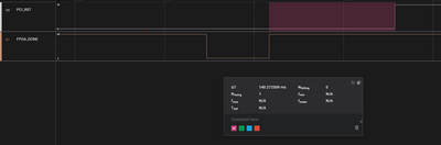
Next step is to implement part of the FBI<->RAMDAC communication (not video data) and clock generation in the FPGA. The FBIs need to read and write quite a couple of registers to configure the VIDCLK and MEMCLK.
The FBI doesn't talk to the RAMDAC at all during system start-up, only when an application is loaded (with some drivers it might configure it when the driver is loaded).
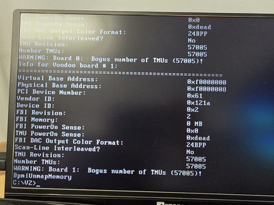
I did some captures on a regular V2:
A snippet:
If anyone is curious, here I have uploaded full captures made when starting a 3D application and when closing it:
http://sdz-mods.com/wp-content/uploads/2024/0 … 0_APP_START.zip
http://sdz-mods.com/wp-content/uploads/2024/0 … 0_APP_CLOSE.zip
These can be opened in the Logic software from Saleae, free download.
I also attached a txt file with the decoded data to this post.
Wow this is a cool project!!
Thanks!
Some more details about this, if anyone is interested.
The RAMDAC has two clock outputs, CLK0 and CLK1.
CLK0 is the FBI VIDCLK, this is dependent on the resolution and refresh rate.
50.35MHz for 640x480@60Hz
80MHz for 800x600@60Hz
65Mhz for 1024x768@60Hz
These clocks are different for higher refresh rates.
The unitialized default clock is 25.175MHz or 31.5MHz.
CLK1 is the FBI & TMU MEMCLK. This is set to 90MHz (usually) while an application is running, 30MHz after stopping said application. For a brief time while the application is started, this clock is set to 16MHz, while it appears that the FBI and TMUs count the memory. The unitialized default clock is 45MHz.
The RAMDAC (ICS5342) has a couple of default frequncies for each CLK, and the PLL parameters for each of these can be changed by the FBI.
CLK0 (VIDCLK) has:
f0 25.175MHz
f1 28.322MHz
f2 31.500MHz
f3 36.00MHz
f4 40.00MHz
f5 44.889MHz
f6 65.00MHz
f7 75.00MHz
The PLL parameters for each of these selectable clocks can be changed and any of the these can be chosen as an output frequency from the PLL Control Register.
CLK1 (MEMCLK) has:
fA 45.00MHz
fB 55.00MHz
Same applies to CLK1 as for PLL parameters and output.
Now, as for what the FBI actually does when initializing the RAMDAC, when 800x600@60Hz is set:
1. Reads PLL parameter register 0B, which corresponds to CLK1 fB.
CLK1 fB is never actually set or used as an output.
2. Reads PLL parameter register 01, which corresponds to CLK0 f1.
CLK0 f1 is never actually set or used as an output.
3. Reads PLL parameter register 07, which corresponds to CLK0 f7.
CLK0 f7 is never actually set or used as an output.
4. It reads the PLL Control Register (0E).
The default values that are in this register are then again written by the FBI a couple of times, later on.
5. Sets PLL parameter register A, which corresponds to CLK1 fA.
This is set as 15.97MHz while, I assume, the FBI and TMUs count the memory (there is a short burst of activity on the RAM data pins while this clock is set).
6. Sets the PLL Control Register (0E) to the values it already had in it...
7. Reads the PLL Control Register (0E)....
8. Sets PLL parameter register A, which corresponds to CLK1 fA.
This is set as 89.99MHz.
9. Sets the PLL Control Register (0E) to the values it already had in it...
10. Writes a command to set :
24-bit True Color With Bypass (True Color)
2X CLOCK CYCLES / PIXEL BITS
24-Bit Direct Color Word - Mode 7
11. Reads the PLL Control Register (0E)....
12. Sets PLL parameter register 0, which corresponds to CLK0 f0.
This is set as 80.05MHz.
13. Sets the PLL Control Register (0E) to the values it already had in it...
The output clocks are CLK0 f0 and CLK1 fA. These are never changed in the PLL Control Register.
Now to test different resolutions and refresh rates and see if it behaves similarly.
Congratulations SDZ!!
How did you even make the circuit board?? 3D printer ??
What about the drivers? Do you perhaps have contact with a former 3dfx employee, which would make this possible? 🤔
If the part is not just a technology experiment and you actually have the card running:
Are there demos that you can show?? 🤔 Otherwise as I said - great work. You have to be a clever person to even be able to implement this.
Regards Aqua 😉
Am5x86 PCI 3dfx Voodoo1.
AMD K6-2 500 3dfx Voodoo2 SLI.
Toshiba P200MMX PC Card Wonder.
Dell Optiplex Small PC Intel Core Duo.
Dell Vostro 1000 AMD64 X2 LD-52.
What's about FSAA X-Factor ?? 🤔
Am5x86 PCI 3dfx Voodoo1.
AMD K6-2 500 3dfx Voodoo2 SLI.
Toshiba P200MMX PC Card Wonder.
Dell Optiplex Small PC Intel Core Duo.
Dell Vostro 1000 AMD64 X2 LD-52.
Extremely cool project! Looking forward to have a look at the files myself. Keep it up!
@Aqua
Thanks!
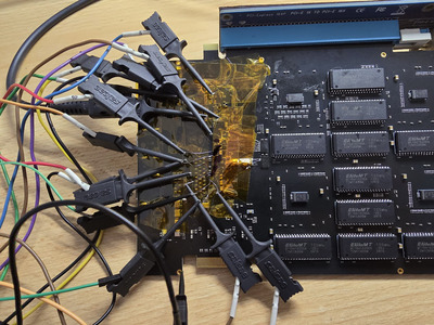
The PCB is made at a PCB factory. While I've seen various PCB 3D printer prototypes, such a PCB can't be manufactured with one.
Due to my OCD, I needed to have all the 3dfx ICs on top and all of them looking symmetrical. The FBI doesn't really want to have the memory arranged as the TMUs. Also, there are a lot of internal parallel buses, which are also high speed and need a ground reference. All of this required quite a bit of routing layers. There are also quite a few traces that need to have controlled impedance.
This is not a 2 layer board 😀
As for drivers, it would need custom ones for the extra TMU, or for making a brick from these cards. Otherwise, it should work fine with the existing V2 drivers.
Sadly I don't know any ex 3dfx employees.
The card isn't running yet, the two Voodoos are detected, drivers can be installed, but that's it at the moment. I need to implement the RAMDACs functionality in the FPGA and the video output.
As for AA, I haven't thought about it yet.
@technokater
Thanks!
sdz wrote on 2024-01-18, 19:38:@Aqua Thanks! The PCB is made at a PCB factory. While I've seen various PCB 3D printer prototypes, such a PCB can't be manufactu […]
@Aqua
Thanks!
The PCB is made at a PCB factory. While I've seen various PCB 3D printer prototypes, such a PCB can't be manufactured with one.
Due to my OCD, I needed to have all the 3dfx ICs on top and all of them looking symmetrical. The FBI doesn't really want to have the memory arranged as the TMUs. Also, there are a lot of internal parallel buses, which are also high speed and need a ground reference. All of this required quite a bit of routing layers. There are also quite a few traces that need to have controlled impedance.
This is not a 2 layer board 😀As for drivers, it would need custom ones for the extra TMU, or for making a brick from these cards. Otherwise, it should work fine with the existing V2 drivers.
Sadly I don't know any ex 3dfx employees.The card isn't running yet, the two Voodoos are detected, drivers can be installed, but that's it at the moment. I need to implement the RAMDACs functionality in the FPGA and the video output.
As for AA, I haven't thought about it yet.
@technokater
Thanks!
Sdz, this is amazing. I come from the drone world where people make their own flight controllers on little PCBs but what you’re doing is next level. May I ask what your day job is? Where did you get all this knowledge?
@zuldan
Thanks!
I design hardware. Mostly complex and high speed systems (CPUs, DDR5, 2000+ pins FPGAs etc).
As for knowledge, aquired over time. There isn't really a single book that has everything in it.
You are basically recreating part of Quantum stuff. Very cool that it is heading for us to use instead of rare Quantum stuff.
Cheers,
Great Northern aka Canada.
I wonder how many seconds per frame this will get in Q3DM11. 😀
@pentiumspeed
Not really a Q3D clone, but it similar in some aspects. Also I wouldn't have sanded down a Q3D card 😀
@leileilol
Hopefully not too many 😁 .
I resumed working on this a couple of days ago.
First, a clarification of my previous post where I described the RAMDAC initialization sequence.
At some point the FBI reads various PLL registers for clock that are never initialized or used. It does this to detect the RAMDAC model installed on the V2 card (ICS, TI etc).
1.First issue to solve was to make mojo actually detect the card under DOS. While it would list fine in windows, under DOS mojo would just freeze the system.
This turned out to be a power sequencing issue, the FBI has config straps on the memory interface, which pull those lines to GND or 5V, while the FBI is powered by 3.45V.
I had the 3.45V rail turning on before the 5V rail, but both were turned on way before the FBI was pulled from reset (by the PCIe to PCI bridge).
After I tweaked the order and timings a bit, both cards are detected by mojo.exe:
2.Next step is emulating the RAMDAC behaviour inside the FPGA. A friend helped me by implementing the state machine, so if everything is OK, mojo.exe should detect the RAMDAC model type, in this case ICS.
It didn't work first try, so further debugging was needed:
After fixing some timing issues, the FBI would correctly detect the RAMDAC type, but not instantly. It would read the same registers quite a few times, and while on the logic analyzer the data coming out from the FPGA looked fine, the data received by the FBI (as reported in the text log file by mojo) had errors.
The FBI is powered by a 3.45V rail, and so is the FPGA bank that is connected to it. However, level shifters were needed in between, because the same pins that are used by the FBI to configure the RAMDAC are also used by the FBI to talk to the RAM. The RAM is powered by 5V, so to avoid sending 5V into the FPGA, level shifters were used. Initially these were configured for 3.45V on the FPGA side and 3.45V on the FBI side. Luckily, I had a resistor option to power this side from 5V, and after making the change, the FBI would always receive the correct data from the FPGA.
This made me wonder, if the FBI is powered by 3.45V, but 3.45V signaling isn't enough, what other signals could be affected by this? The most important ones are the 3 TMU memory clocks, 1 FBI memory clock, and 1 FBI video clock.
On a regular Voodoo2 card these signals come from the RAMDAC (which is also powered by 5V, so probably 5V amplitude, I haven't checked) and feed into a buffer, usually a 74AC244. This buffer is also powered by 5V.
For a quick test, I took a regular V2 card, lifted pin 20 of the 74AC244 IC (VCC PIN) and connected it to the FBI power rail (3.45V). I then ran mojo. exe and it could successfully detect the FBI, TMUs and RAM.
So I thought this would not be a problem, we'll come to this back later.
3. After thinking that the 3.45V clocks would be OK, I quickly generated inside the FPGA a 16MHz FBI/TMU memory clock (this is how the memory clock is set for a regular V2 card for counting FBI/TMU memory but also for FBI<->TMU communication).
Running mojo. exe would just do this:
Checking the mojo.exe log:
"Resetting TMUs after clock change
Could not reset TMUs..."
Checked the schematic again, all seemed fine. The only possible issue I could think of was the 3rd TMU, so I disabled it in hardware. After doing this:
I did some further tests with mojo on a regular V2 card. If the second TMU is disabled, it gives the same error as before. So it's quite possible that if mojo. exe doesn't detect exactly 2TMUs installed, it just quits and throws that error.
For now, I'll just leave the 3rd TMU disabled on both "cards".
4. Now that the FBIs talk to the TMUs and correctly report the memory, I removed the hardcoded 16MHz memclk and 40MHz vidclk I added previously, and configured the FPGA so that is outputs whatever clocks the FBI asks for (well, at least for 800x600 for now).
Booted in windows, ran donut. exe and instant "Don't send error". Probing the memclk and vidclk showed no change while the application was started. Default memclk is 30MHz, and it should go to 16MHz for a bit while the FBI/TMU count the memory, and then go to the regular 90MHz clock. The default vidclk was set to 45MHz and it should go to 80MHz for 800x600@60Hz.
Then I probed the RAMDAC again, and there was no activity from the FBI. No configuration was done. I thought maybe it was SLI related, disabled half of the board and removed various pull-up, pull-down resistors. Same error.
I then removed the card and added the regular V2 card I used before for testing, and it would instantly throw the same error. After reinstalling the driver no more error, but the application would just hang.
This card still had the 74AC244 powered by 3.45V instead of 5V. After I reverted this it started working properly.
I then tested with my card and the reinstalled drivers, and sure enough, no more instant crash, but the application would hang. I could see that the FBI configures the "RAMDAC" and is fed the correct clocks.
So it appears that while the FBI/TMUs work with a 16MHz 3.45V clock, they don't work with a 90MHz/80MHz 3.45V clock (3.45V and 5V ignoring any ringing/overshoots etc).
This also explains why I never got a regular V2 card running through a PCIe to PCI bridge, when the VCCIO on the PCI side is set to 3.3V instead of 5V.
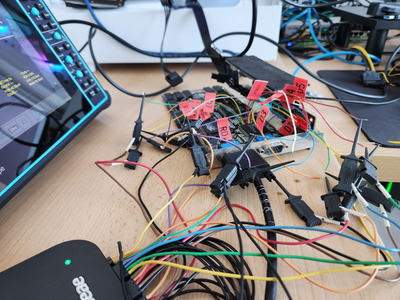
Time to bodge in some gates/buffers.
I found some SN74LVC1G17 schmitt triggers, bodged them in and buffered the memory clock for the two TMUs and FBI, and the FBI vdeo clock.
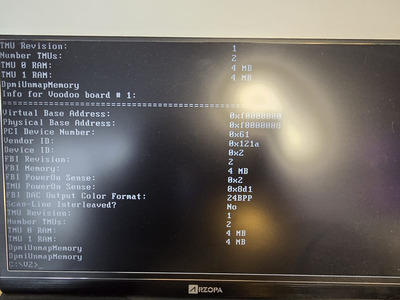
The application would still hang and there was no activity on any FBI/TMU RAM bus. After that I disabled in the registry both TMUs, and the application wouldn't hang. Enabled the first TMU, it still worked and there was activity on the FBI and TMU0 RAM address/data pins.
Found a short on two pins of one of the RAM ICs connected to the second TMU, removed that, and now the FBI and both TMUs run.
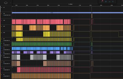
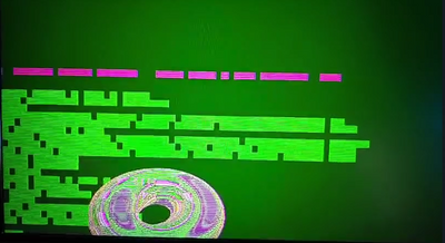
This is the video data coming out of the FBI IC, going into the FPGA.
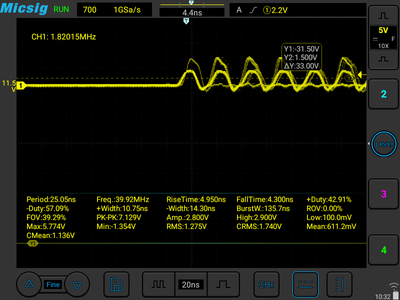
Would you look at that sweet 3dfx donut 😀
Edit: I'm not sure at the moment if it will work without those buffers, but I'll leave them in for now.
Edit2:
Time for an update. Some good news and some bad news.
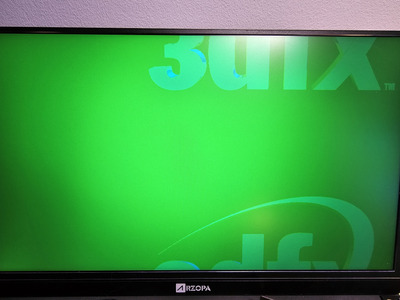
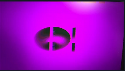
I am now able to get a properly alligned image out of the V2 4444SX, however the colors are still wrong:
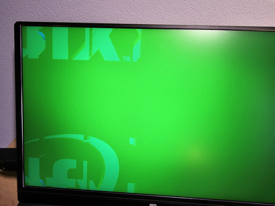
And sometimes this happens:
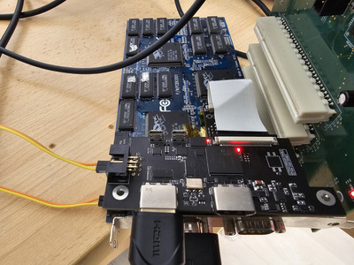
Also, master FBI now has 1 dead pin, as well as the FPGA. I had to solder quite a few wires to debug things, and the one connected to the blanking signal shorted probably to the 12V rail.
At the moment the card is running with the FBI on the right, as that has a separate blanking pin routed to the FPGA.
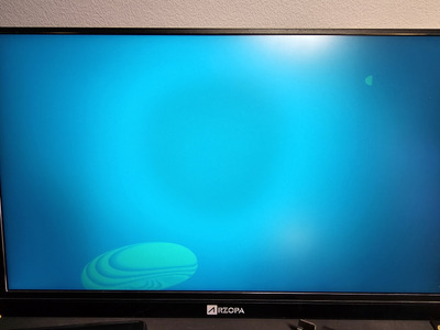
As for the good news. To help debugging the video output, I ported part of the code on this:
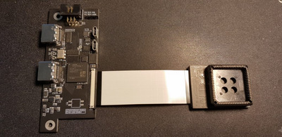
And finally got V2 HDMI output from it 😀
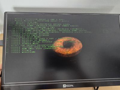
The picture doesn't do it justice. Compared to the VGA output (my LCD VGA monitor and cable surely arent't the best, but so is the HDMI display I use for testing) the image is stable, there is no noise and no artifacting. The colors are really crisp and vibrant. I'll try to get a proper HDMI capture card and record some gameplay, but this is by far the best output I ever got from a V2 card.
On this addon card I'm deriving all the internal clocks from the VIDCLK fed by the FBI. The MMCMs had some issues locking as the FBI was providing the clock only when running something, and the MMCMs were starting without an input clock. I was able to fix that and now it relocks every time.
On the V2 4444SX, I was using the internal generated VIDCLK as a reference (which was fed into the FBI and fed back from it into the FPGA). I checked and there appeared to be no phase difference, but it's possible the clock is delayed with a period multiple. I'll port the changes to it and see if the colors look any better.
Love hearing about the development of this card. Each step of the process is a fantastic insight into hardware/software development process. Please continue to post updates 😀
If you can do that surely someone is able to do some new 3dfx replications for the retro players rather than collectors