In terms of being able to reach 386 speed, yes the P3 solution does work.
However I feel that with the Socket 7 solution there are quite a few benefits.
I wasn't able to reach the speed of a faster 386 or a slower 486. The disabled cache just cripples the performance to much. I also found that most P3s and Celerons don't have an unlocked multi, meaning there is only so much flexibility. When I started this project I never thought that you need a 1 GHz chip to reach 386 speeds. I was quite shocked by the result because I know that a 486DX2 66 with cache disabled gives you a perfect 386. So I guess the architectures are just way to different and it seems the closer you are to 386 hardware in terms of age, the easier it is to use the L1 cache trick 😀
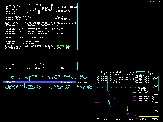
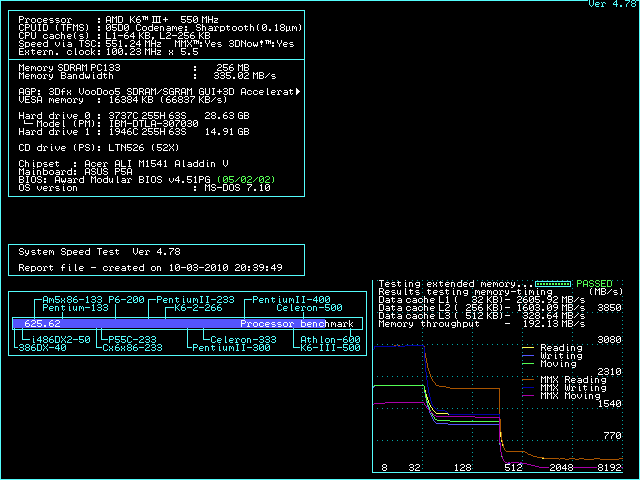
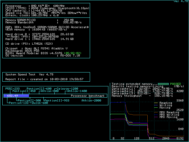
Initial tests on the Super Socket 7 platform has shown me that you can easily reach the speed of a 386DX 40 and go even faster. Changing the multi is very easy on these boards as well and there is a wide range of cpus from a Pentium 133 to K6 550 and a few Cyrix chips.
Most of the benefits remain:
Easy to obtain
Cheap
BIOS, Drivers, Manuals directly on the manufacturer website
ATX compatible
Button type batteries
2-3 ISA slots on pretty much every board
AGP slot
So in a nutshell, yes the P3 project was a success but I believe the Super Socket 7 board will give me better results and greater flexibility, being able to cover a much wider "target speed" range...
On Super Socket 7 boards, tests have also shown that L2 cache does have an impact (L2 cache had zero impact on the L3 platform.
Armed with tweaking options for L1 and L2 cache, unlocked multipliers and a wide range of cpus, this project should become a huge success!
EDIT: I also ordered that ATX to AT adapter with switch. You posted it a while ago with a link on ebay. If that gadget works as advertised I might soon be playing with real 386 / 486 hardware as well 😀
EDIT EDIT: And it's about the journey not the destination 😁