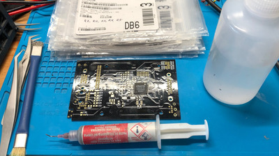
I hate to always dominate this thread, but here is where I’m at today. Plan on doing just the tiny SMD components on SN9. Save the pin headers and other larger stuff to Monday.
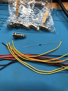
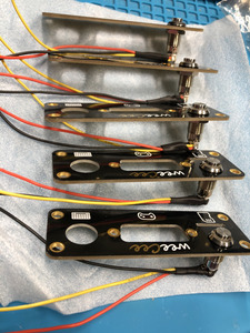
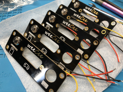
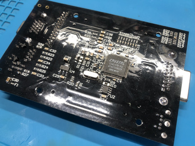
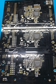
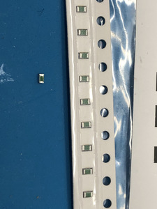
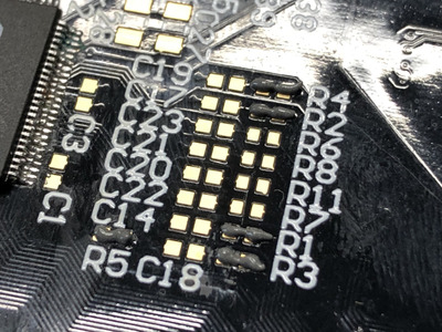
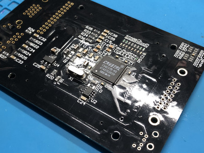
Also showing the remaining boards, and how it feels to start out. To streamline the process I have the bags pre-sorted to do tiniest parts (starting with resistors then caps) on to the larger ones. Each bag has the pad numbers listed on it. The boards have the crystal chip already pre-installed, as that is an entire affair by itself.
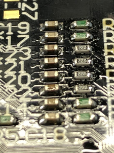
Honestly I turn on some tunes and point a fan at me and zone out on it. Just remember to use the right amount of solder paste, flux where needed, and if you need to even out the solder blobs on either side of any SMD component, just drag both sides over the two different pads to try and even out how much solder is on each side of the component. That will help keep it from one side having more than the other (just try not to knock against other neighboring components while doing so). And if you find you’re burning yourself, use some gloves, heat resistant ones if you can.
In case you get too much solder on any pad, you can always put some solder wick on it to “vacuum” up any extra solder, just remember to use a light touch.
With soldering it’s about getting the heat up to where you need it, doing what you need done fast, and then getting the heat off the soldering area. The time that heat is on pad is the biggest factor in burning pads, not necessarily the heat’s temperature value. So when soldering, it’s best to get the heat up, spend as little time as needed to get things set together, and then remove heat.
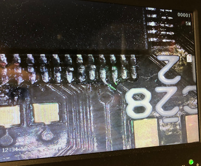
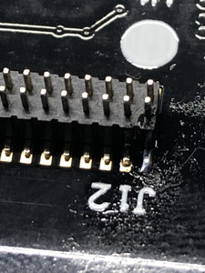
Anyways, it’s impossible to not mess something up (known as a production defect), as it’s impossible to not knick against the thin outer insulating coating of these on-demand manufactured PCBs. Isn’t the first time I’ve had to use some solder mask to “fix” problematic areas.
On the microscope is one such area on SN9’s audio chip, where one of the contact pads was dislodged after trying to move it back after it had been pushed too hard. It wound up tearing the contact pad slightly off the wafer (run still attached), which is fine since it’s easy to glue it back down with some solder mask.
Still, makes me sad when something like that happens, as I’ve been told by many folk that I’m looking far too into it. If it works in the end, who cares? Well, I try my best, but imperfections like this are unavoidable during hand made production. It takes a lot of years of experience to get good at this stuff, and we’re talking about making a small number of them for people’s curiosity. No way you’re going to get a perfect unit, with perfect solder work on each and every connector.
Regardless, I like to be transparent about these things. If someone asks I’ll gladly point out how it doesn’t affect function. In fact, I chose to use more copper in the main boards of these anyways (which costs extra), maybe they just needed some more time on the machine for the black coating to deposit but, who knows.