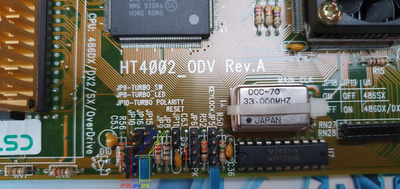
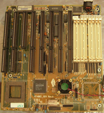
JP9 is meant to be connected to a turbo switch. In some cases, the switch is open when the turbo button is "active", in other cases, the switch is closed when the turbo button is active (and there are cases that have a three-pin turbo switch connector, and the switch switches whether 1-2 or 2-3 is connected). I wonder why JP10 has three positions and is not plugged at all. You only need to choose between "turbo is when the switch is open" and "turbo is when the switch is closed", which would usually be implemented as a 3-pin jumper to be toggled between 1-2 or 2-3, or 2-pin jumper that will be set or not. You can just try how the board reacts to JP9 in the three possible configurations of JP10.
Keylock/Power LED is usually combined into a single 5-pin connector, in your case it is JP5. I have no idea what JP15/JP16 are supposed to do on your board.
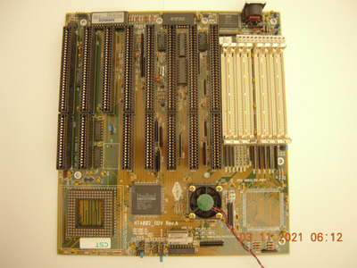
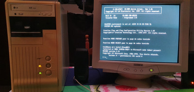
It seems a battery has been removed from that board. This is a good idea, because most of these batteries start to leak and corrode the board. But that also means the board won't be able to keep time and settings when it is powered off, as there is no replacement power source installed.
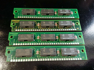
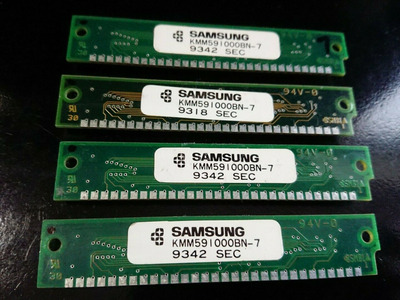
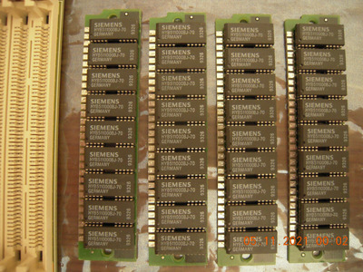
Furthermore your board doesn't have any L2 cache. I looked up the HTK340 chipset, consisting of the HTK321 ISA bridge and the HTK320 memory controller (the latter has a fan on your board), and the manufacturer claims that the memory interface is performance-optimized in a way that the system is "fast enough without L2 cache in most usage scenarios". I don't doubt the claim that the board has a high-performance memory interface, and the write-merging write buffer built into that chipset will (if designed correctly) indeed help a lot with typical memory access patterns by 16-bit software that otherwise would be handled by the L2 chace. The chipset can do bank interleaving on the DRAM. I strongly recommend you make use of that option, i.e. you plug in 8 identical 30-pin SIMMs, either 8*1MB = 8MB total or 8*4MB = 32MB total.