VOGONS


First post, by Return 0;

User metadata
Rank Newbie
Rank
Newbie

Hi,

In this thread I would like to introduce a cache memory design for the 486 and other computers using 5V asynchronous CMOS SRAM.

The problem for me was to find memory faster than 15ns in a PDIP housing that is not a scam, so the solution is to make them yourself from components currently available in stores.

It worked, I just finished the tests successfully.
The files are ready to make the PCB in an external company, I used JLCPCB.
How to do it? Here is the answer:
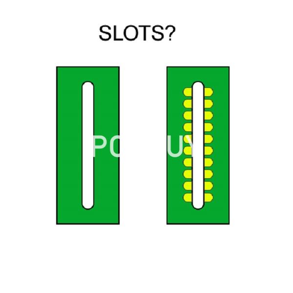
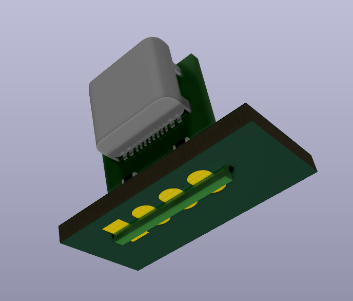
- please solder the socket with the PCB (cacheIC.zip) and 3x goldpin 2.54mm 16PIN header
-please solder socket PCB with PCB cache (cache.zip/cache64.zip)
-Please solder the SRAM chip.

Memories that can be built:
128kbx8=128kB, I used PCB cache.zip and IS61C1024AL-12JLI SOJ32 chip (128kx8 12ns, 5V CMOS SRAM)
but may be different with pinout compatible SOJ32 CMOS 5V SRAM e.g. 10ns.

64kbx8=64kB, I used for this purpose PCB cache64.zip and AS7C1026B-10TCN TSOP II 44 chip (64kx16 10ns, 5V CMOS SRAM)
but may be different with pinout compatible TSOP II 44 64kx16 CMOS 5V SRAM eg 12ns.

32kbx8=32kB, I used for this purpose PCB cache.zip and CY7C199D-10VXI SOJ28 chip (32kx8 10ns, 5V CMOS SRAM)
but they may be different with pinout compatible SOJ28 CMOS 5V SRAM, e.g. from another manufacturer.
In this case, please solder the chip from the first pin according to the marking on the PCB, the last 2 rows of pins hang in the air.
EDIT! I added a PCB specifically for 32x8, you can use it instead of the above method (cache32.zip and cacheIC32.zip) EDIT!

In the case of soldering cache.zip sockets as in the pictures, the marker on the chip is the marker in the cache socket of the motherboard and this side should be placed.

In the case of soldering cache64.zip sockets as in the picture, the tag on the chip is on the opposite side of the tag in the cache socket of the motherboard.

The entire project is available for free, please feel free to use it.
If you want to support my hobby, you can do it via paypal: onlytimecansaveus@gmail.com

IMG-2766.jpg
IMG-2767.jpg
IMG-2768.jpg
IMG-2763.jpg
IMG-2762.jpg
IMG-2764.jpg
IMG-2765.jpg
IMG-2755.jpg
IMG-2756.jpg
IMG-2754.jpg

Last edited by Return 0; on 2023-08-11, 11:40. Edited 2 times in total.

Reply 1 of 7, by GigAHerZ

User metadata
Rank Oldbie
Rank
Oldbie

Now, that is cool!

"640K ought to be enough for anybody." - And i intend to get every last bit out of it even after loading every damn driver!

Reply 3 of 7, by rasz_pl

User metadata
Rank l33t
Rank
l33t

Async cache for Pentium was a scam, and often lowered performance (Quake). Here with Overdrive and half the fsb its probably actually beneficial.
Im surprised those 2 layer boards work, especially 64 one 😮 40MHz with parallel tracks passing different 5V signals on top of each other and no ground planes, and no bypass capacitors 😳, and floating data pins. Would be interesting seeing if this works on socket 5 at 66MHz.
Were you able to set fastest cache options in Hot433 bios?

Great job taking the initiative and making something!

Open Source AT&T Globalyst/NCR/FIC 486-GAC-2 proprietary Cache Module reproduction

Reply 4 of 7, by mkarcher

User metadata
Rank l33t
Rank
l33t

Great idea! Thanks for sharing your boards. You might want to add solder pads for a 100n bypass cap close to the chips, especially in the 64k x 16 variant in which you already have a GND and a +5V trace close together near the power pins in the center of the IC.

I'm in the process of publishing the complete design sources of my first go at the Biostar Cache module soon, too, but this approach is obviously more versatile.

Reply 6 of 7, by DerBaum

User metadata
Rank Oldbie
Rank
Oldbie

Here is an idea to further reduce the complexity.
You could work with a slot where you slot in the second circuit board and eliminate half of the pins needed and reduce the solder joints by 30 percent... You directly solder Board to board.
I have seen this type of construction inside several cheap chinese toys... But i always thought the idea of slotting boards into each other like this is brilliant.

https://www.pcbbuy.com/news/What-is-Slot-in-P … ng-Process.html
44555_2021120609341298849053.jpg

https://forum.kicad.info/t/footprint-for-daug … st-method/26396
11af94f9ddd0567c83497ada9845d8e26e3e9e2d.png

FCKGW-RHQQ2

Reply 7 of 7, by pentiumspeed

User metadata
Rank l33t
Rank
l33t

Didn't thought of this way. Thank you. I had hard time finding a solution that meets 2 requirements: zero clearance between dip outline and low profile for SOJ IC assembled and soldered to the board. Needs to have 4 layers for best capacitor bypass. No place for bypass capacitors except under IC or on bottom of the adapter board.

1MB x 1bit DRAM ICs are nearly impossible to find in DIP package. Lots of this in SOJ package through.

Cheers,

Great Northern aka Canada.