VOGONS


First post, by Thermalwrong

User metadata
Rank Oldbie
Rank
Oldbie

The Voodoo 1 was the first 3d accelerator I had, I skipped the Voodoo2 so the Voodoo 1 is the one I have more interest in - I still don't have enough Voodoo II for an SLI setup as well 😉

It seems that unlike the Voodoo 3 and perhaps the Banshee, there's very little definitive information on the Voodoo 1 and Voodoo 2. Which is odd since they were manufactured by so many different vendors prior to the STB buyout, there's probably an information pack out there somewhere.

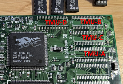
I've got a few 3Dfx Voodoo 1 cards, because I keep buying broken ones with the hope of getting lucky or fixing one. So far I've had some success but there are 2x Voodoo1 cards that I've not yet been able to fix which are showing black blocks or lines in textures in games like the Tomb raider demo - this is after making very sure that every pin from the TMU is attached, but games look fine if I enter the environment variable to turn off texture mapping.

I decided to look around for schematics or a pinout for the Voodoo 1 or Voodoo2 but there doesn't seem to be one that's immediately available. Then I remembered that 3Dfx chips and cards made their way into many arcade machines and those systems cost enough that you'll usually find schematics for repairs during their operational lifetime. In particular Midway were quite fond of 3Dfx and the Midway Seattle both uses 3Dfx's Obsidian graphics engine and has available schematics. Search for "Midway_Seattle_Hardware_Schematics.pdf" to have a read.
I've split out the 3Dfx related part which starts with "THE OBSIDIAN GRAPHICS SYSTEM BLOCK DIAGRAM". Please note that these are a PDF of a PDF of scanned pages, see the full document's pages 42 to 56 in the PDF for the original print quality.

Filename
Obsidian-GE-Schematic-Voodoo1-FBI-RAMDAC_compressed.pdf
File size
2.69 MiB
Downloads
90 downloads
File license
Fair use/fair dealing exception
Filename
Obsidian-GE-Schematic-Voodoo1-TMU-BYPASSCAPS_compressed.pdf
File size
3.38 MiB
Downloads
72 downloads
File license
Fair use/fair dealing exception

I don't think the system itself is very similar to an x86 PC but the 3Dfx part is all PCI. There are some minor differences, notably the video output will have no need for 2D input / switching but that's not too important.
If you enable the debug file output as an autoexec variable:

set SST_INITDEBUG_FILE=sst.log

And then run the diagnostic tool mojo.exe, the SST.log file contains this reference to Obsidian GE:

sst1DeviceInfo: Board ID: Obsidian GE
sst1DeviceInfo: FbiConfig:0x2, TmuConfig:0x11
sst1DeviceInfo: FBI Revision:2, TMU Revison:1, Num TMUs:1
sst1DeviceInfo: FBI Memory:2, TMU[0] Memory:2
sst1DeviceInfo: Dac Type: TI TVP3409
sst1DeviceInfo: SliDetect:0

Something I find quite interesting is that there are 3x 16-bit wide buses for chip to chip communication, I was wondering how this was laid out:
FT_ADDR 0 to 2 (up to 4 possible addresses...)
FT_DATA 0 to 15 - I think this is FBI > TMU data
TF_DATA 0 to 15 - I think this would be output from the TMU to FBI
TT_DATA 0 to 15 - This should be for TMU > TMU communication I think???, these pins are all grouped up on a regular Voodoo 1 since it's not doing multitexturing 😀
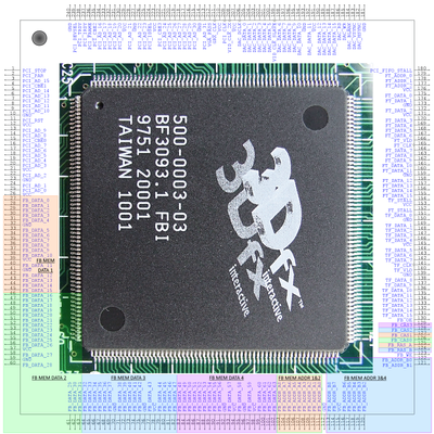
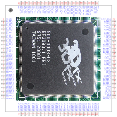
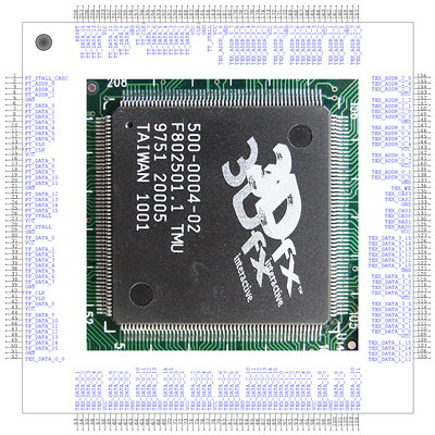
From the schematic information which lists full pinouts for both the 3Dfx 500-0004-02 TMU and 3Dfx 500-0003-03 FBI, I've put together an initial pinout for the TMU which matches up very well with what I see on the PCB:

3DFX_500-0004-02_TMU.png
Filename
3DFX_500-0004-02_TMU.png
File size
715.21 KiB
Views
1962 views
File license
Fair use/fair dealing exception

The memory bus is taking up most of the pins on the TMU, it's got a 64-bit wide memory bus dedicated to the TMU, with individual control of all address and data bits for each of the 4x memory chips, only grouping up the RAS pins. I think going by the numbers the memory layout should be like this - here's the other card I'm trying to fix:

500-0004-02_TMU_MemLayout.jpg
Filename
500-0004-02_TMU_MemLayout.jpg
File size
481.89 KiB
Views
2089 views
File license
Fair use/fair dealing exception

Going from what I've read about the Voodoo 1 going to the Voodoo2, with the V2 mostly getting speed improvements from being a process improved, better optioned version of the Voodoo 1, giving it higher clocks and multitexturing.
I suspect that the TMU chips may have a lot in common beyond just the pin count (208 on V1 and V2) although someone would need to check, specifically the TT_DATA pins would be important to verify first.

Soon I'll do the same for the FBI chip 😀

edit: edited to replace the lossy jpeg pinout diagram with a lossless one.

Last edited by Thermalwrong on 2023-11-15, 18:01. Edited 2 times in total.

Reply 1 of 13, by sdz

User metadata
Rank Member
Rank
Member

Checking those arcade schematics is just brilliant, it never occured to me, thank you!
This will prove quite useful if I ever decide to do with the OG Voodoo chipset what I'm doing with the V2, saves countless hours of sanding the pcb, scanning, retracing and getting a schematic.

As for the V2 TMU, I randomly compared about 30 pins, and they are identical to the
500-0004-02. I'll check all the pins and give an update later today.
Edit: All V2 TMU (500-0010-01) pins are identical to the V1 TMU (500-0004-02). This could prove to be quite interesting...

Regarding the TT bus, you are right.
A V2 looks like this:
FBI to TMU0 and FBI to TMU1 (same nets but the bus is split), this is the FT bus.
TT bus (from TMU1 to TMU0)
FT bus (from TMU0 to FBI).

Basically the TMU outputs are daisy chained back to FBI input.

Reply 2 of 13, by Thermalwrong

User metadata
Rank Oldbie
Rank
Oldbie

Wow, thank you for checking that, that's amazing that the pinout is the same 😀
That's quite interesting that the TT bus is potentially just used to send the TMU's data back to the frame buffer and the FT bus is shared - that must be why there are FT address pins, to address data to each of the TMUs?

I've now done the same treatment for the 3Dfx 500-0003-03 FBI chip. This one's a bit different in how it addresses memory, there are only two sets of memory addressing pins and the notation for the framebuffer memory data pins doesn't clarify which set of FB_DATA pins goes to which memory chip. So I've clarified the picture with a colour highlight for each memory chip - the boxes with two colours are the pins shared between two memory chips.

Here's the colourised version:

3DFX_500-0003-03_FBI-channels.png
Filename
3DFX_500-0003-03_FBI-channels.png
File size
946.73 KiB
Views
1963 views
File license
Fair use/fair dealing exception

And the unannotated version:

3DFX_500-0003-03_FBI.png
Filename
3DFX_500-0003-03_FBI.png
File size
1.06 MiB
Views
1984 views
File license
Fair use/fair dealing exception

They're losslessly compressed this time 😀
Unfortunately this is where the Voodoo 1 differs from the Voodoo2 - the 500-0003-03 FBI chip has 240 pins while the 500-0009-01 CK or 'Chuck' has 256 in total. I do wonder if the pins would be the same up to pin 240 and then they added in some extra pins, or if it's all different.

Reply 3 of 13, by sdz

User metadata
Rank Member
Rank
Member

Yes, you're right, that's why the FT has address pins. Each TMU has a few config resistors (hanging on the RAM bus, address pins if I recall correctly), that's how the TMU address is set, among other things.

In a day or two I'll post a delta between the two FBI ICs.
Btw, the OG Voodoo Graphics can have up to 3 TMUs and supports SLI, eg. Primary Image Pirahna IIRC.(if it's not that it's the Barracuda, although I think that uses the V2 chipset).

Reply 4 of 13, by sdz

User metadata
Rank Member
Rank
Member

I compared the pinouts, the V2 FBI has the following extra pins:
- 2 extra RAS lines
- PCI INT pin
- SLI SYNC signals (2x)
- a reset signal that goes to the TMUs (buffered from PCI RST)
- a clock signal that goes to the SLI slave
- a pin for sensing if the card has a monitor plugged in, goes to the RAMDAC which detects the 75R VGA terminations (this is how 1 card becomes the master in an SLI setup).

Reply 5 of 13, by Thermalwrong

User metadata
Rank Oldbie
Rank
Oldbie

If you give me a potential pinout I can make an initial pinout picture for you 😀 Just 16 pins between the two

I am trying to figure out why my Orchid Righteous 3D only sees 1MB on the TMU when I can't see any bad pins. I am wondering if perhaps I reconfigured one of the strap resistors - I did most of the work on this faulty card in 2021-ish, before I kept reliable logs of changes I make to each item.

Those additions for SLI / function make sense, as far as I'm aware the 3Dfx FBI chip has little the in way of GPIO type pins to assign extra functions to. Makes Anthony's King Shaman 3Dfx Voodoo 1 card quite impressive at a hardware level 😀

Reply 6 of 13, by Thermalwrong

User metadata
Rank Oldbie
Rank
Oldbie

Wow, 18 months ago I forgot I made this picture when I was first troubleshooting my £20 trainwreck Voodoo 1 reference design card:

3dfx-reference-design-vgaswitch.png
Filename
3dfx-reference-design-vgaswitch.png
File size
217.75 KiB
Views
1713 views
File license
CC-BY-4.0

This is from the PI5C-3384Q datasheet since that's one of the first parts I was fixing. Should be the same on most designs that use this small 24-pin chip to switch between the two VGA sources like a KVM 😀

Most Voodoo 1 cards use resistors and resistor packs to connect up the memory data / address / RAS / CAS lines and if you've watched any 3Dfx repair videos you'll know those can be at fault too. I was trying to figure out what caused the black blocks on textures on my reference Voodoo 1 and through chance tracked it to the one resistor pack that connects up TMU memory on this cheaply made card (nicer cards will use resistor packs for everything):
Re: What retro activity did you get up to today?
One solder joint went bad on this resistor pack, which connected up the CAS (column address select) lines to the TMU memory chips, which broke the cards ability to put data into all of the texture memory even though all the RAM was good.

For troubleshooting memory issues I think it's probably best to start with checking that the RAS & CAS lines are still working. I've made this A4 sized colour printable version of the pinouts which includes the EDO RAM pinout too.
Instead of just checking from each side of the resistor pack, it's best to check from RAM pin to TMU / FBI chip pin, since applying pressure to the resistor pack might make it make a normal connection again.

Attachments

Reply 7 of 13, by Imperious

User metadata
Rank Oldbie
Rank
Oldbie

Thanks for this information.
I had some success repairing my Diamond Monster card earlier this year. There is software You can check the Ram chips but need a PCI card that has expansion slots.

3dfx Voodoo 1 fault diagnosis and repair

I still have a friends card to repair and all RAM chips tested ok. I'll take a closer look at the resistor packs.

Atari 2600, TI994a, Vic20, c64, ZX Spectrum 128, Amstrad CPC464, Atari 65XE, Commodore Plus/4, Amiga 500
PC's from XT 8088, 486, Pentium MMX, K6, Athlon, P3, P4, 775, to current Ryzen 5600x.

Reply 8 of 13, by Thermalwrong

User metadata
Rank Oldbie
Rank
Oldbie
Imperious wrote on 2023-11-22, 00:30:
Thanks for this information. I had some success repairing my Diamond Monster card earlier this year. There is software You can […]
Show full quote

Thanks for this information.
I had some success repairing my Diamond Monster card earlier this year. There is software You can check the Ram chips but need a PCI card that has expansion slots.

3dfx Voodoo 1 fault diagnosis and repair

I still have a friends card to repair and all RAM chips tested ok. I'll take a closer look at the resistor packs.

Ah, your thread inspired me to keep going, thank you for sharing it! 😀
That thread is a great example of what an FBI / frame buffer memory failure looks like - very different from a TMU failure since texture memory doesn't affect overlay like that it, it only affects textures,

Reply 9 of 13, by Thermalwrong

User metadata
Rank Oldbie
Rank
Oldbie

An update - I've repaired a few Voodoo 1 cards now with the reference design which directly connects the memory data & address pins rather than using resistor packs. The main weak point I'm seeing on Voodoo 1 cards is not so much the memory actually failing, but the solder on the legs of the TMU and FBI chips is often detached. That makes sense since those are the most complex parts on the relatively reference layout cards, the two chips are also located in the area that's going to get flexed the most. In comparison, the memory pads are huge and they're not liable to get flexed.
The TMU also seems to benefit greatly from a heatsink, I'm just putting a 40mm flat ceramic heatsink on mine and it makes a difference. *IF* you want to remove a heatsink from a Voodoo 1 / 2 card, please don't pull on the heatsink directly as the QFP legs are not a strong bond to the PCB. Spray or drip some IPA between the heatsink edge and the FBI/TMU chip which should loosen the adhesive, gently wedge a blade in and put in more IPA to break the bond with minimal force. Unless that thermal epoxy stuff was used, then I've got no idea 😜

I'm still working on my Orchid Righteous 3D though which will only see 1MB of TMU memory and has bad texture corruption 🙁 That does have resistor packs to check through each point of.
I don't get the TMU chip, the video memory is surely accessed in 16-bit chunks so why does it map the CAS lines to the Upper CAS of chips 1&2, Lower CAS of chips 1&2, then Upper & Lower CAS of chips 3&4 separately. It seems to use the RAS line as a chip / bank select, which is why the Voodoo 1 TMU memory upgrade mod works.

Anyone with a Voodoo 1 that's not working right here are a few common problems I've come across and the resolution for each:

  • Green screen when starting games in Windows + Crash
    This has been caused on my test PC when installing a Voodoo 1 again after installing drivers for a Voodoo 2. Uninstalling the Voodoo 2 driver, manually clearing all files in the Windows directory that match the files in the V2 driver folder, clearing all 3Dfx registry entries, helped in my case. Then the Voodoo 1 drivers could be reinstalled and they no longer caused a crash. Alternatively just reinstall Windows
  • Display fails to switch over in Windows, displaying background & game window + Seemingly Crashed
    This happened after I installed a heatsink that is liable to have flexed the upper left corner of the FBI chip. That connects the DAC and circuitry to switch over the display. Resoldering that side of the chip with plenty of flux resolved the issue. Beyond that there could be an issue with the 3384Q display switch chip but that's less likely unless there's evidence of an impact in that area.
  • Texture errors - Diamond shaped, Black blocks or noise on textures
    Please note that this is different from lines across the whole of the image, texture errors should look like a normal game but with bad / broken textures which can often include text or backgrounds. The Voodoo cards are 3D only so the menu is a fully 3d rendered image with backgrounds being textures. You can test without textures with the Tomb Raider demo in DOS by entering "set SST_TEXMAP_DISABLE=1" before running the game. If the game looks normal enough with everything white but polygons & the display looks normal, then the fault is texture memory based.
    This seems to be commonly caused by the TMU chip having a detached leg that connects to a memory chip. Resoldering the left, top and right of the TMU chip can often resolve the issue. Be careful to check for solder bridges and use lots of flux. Personally I use an excess of fresh solder to clean the chip legsdrag along the side of the QFP, then suck up or wick off the excess, then make sure that area is still securely soldered.
    Another possibility if that doesn't help, or an alternative to check is the quad 0-ohm resistor pack (RA96) just above the top side of the TMU chip. That connects up the 4x CAS lines to the memory chips and if it's cracked or not attached somehow it can cause completely broken texture memory as well. There's also a 0-ohm resistor (R202) on the back of the reference design card in just about the same location, if that's broken them TMU memory will be completely non-functional.
    The legs / traces connecting the TMU to the FBI are quite unlikely to the problem with texture display issues. A failure of FBI > TMU and TMU > FBI communication usually results in a crash unless texture mapping is disabled, they use a dedicated bus in each direction and missing signals on those lines will cause outright failure instead of glitches. I think?
    After checking each of those things it could be worth replacing the TMU memory, seems rarer for it to fail in my experience though.
  • Crash when trying to run Mojo.exe
    There can be a few things that caused this of course, but here's one I saw where the FBI chip on the card couldn't communicate with the TMU properly, not getting the return data which made it crash the PC. I think there may have been more to it with the file not even getting written before it would crash but I didn't write it down so it's gone 😀
    In my case reflowing the pins that go from the top of the FBI chip to the bottom of the TMU chip resolved the issue.
    Crash when trying to run Mojo

    sst1Init Routines: InitCode $Revision: 8 $
    sst1InitMapBoard(): BoardsInSystem = 1
    sst1InitMapBoard(): vAddr:0xe0000000 pAddr:0xe0000008 Dev:0x9 Board:0
    sst1InitRegisters(): Setting TREX-to-FBI FIFO THRESHOLD to 0x8...
    sst1InitRegisters(): Setting PRELIM FT-CLK delay to 0x8...
    sst1InitRegisters(): Storing TREX0INIT0=0x5441
    sst1InitRegisters(): Storing TREX0INIT1=0xf420
    sst1InitRegisters(): Storing TREX1INIT0=0x5441
    sst1InitRegisters(): Storing TREX1INIT1=0xf420
    sst1InitRegisters(): Storing TREX2INIT0=0x5441
    sst1InitRegisters(): Storing TREX2INIT1=0xf420
    sst1InitRegisters(): Setting up FAST DRAM Configuration
    ERROR: b_sum=0x650 r_sum=0x500
    sst1InitFillDeviceInfo(): Retry #1 for chip GetInfo()...
    ERROR: b_sum=0x650 r_sum=0x500
    sst1InitFillDeviceInfo(): Retry #2 for chip GetInfo()...
    ERROR: b_sum=0x650 r_sum=0x500
    sst1InitFillDeviceInfo(): Retry #3 for chip GetInfo()...
    ERROR: b_sum=0x650 r_sum=0x500
    sst1InitFillDeviceInfo(): Retry #4 for chip GetInfo()...
    ERROR: b_sum=0x650 r_sum=0x500
    sst1InitRegisters(): ERROR filling DeviceInfo...

  • Card not detected
    Make sure the PCI pins are clean and check each of the "FBx" inductors for cracks.
    There are a few of the large dark grey "FB" inductors dotted around the card with many in the left left corner by the RAMDAC. Those are often providing filtering to the power coming into each chip so a cracked inductor can result in important components not being powered. They're also large so if improperly stored then they can be broken off. sdz has determined the proper replacement part here: Re: Diamond 3DFX Voodoo 1 repair
    Beyond that, check or resolder along the bottom and lower-left side of the FBI chip, those are the PCI connections.

I'll add more as I come across them in future. If anyone knows how to troubleshoot noisy / jittery VGA output on a Voodoo 1 / 2 please let me know 😀

Reply 10 of 13, by anthony

User metadata
Rank Member
Rank
Member
Thermalwrong wrote on 2023-11-15, 03:26:

Obsidian-GE-Schematic-Voodoo1-FBI-RAMDAC_compressed.pdfObsidian-GE-Schematic-Voodoo1-TMU-BYPASSCAPS_compressed.pdf

unfortunately these schematics have nasty errors in the fb-tmu connection in tf part. just check by any available photo of any v1 card. those connections are pretty straight-forward.

haven't checked the memory interface, but even if there's all ok real cards may have byte swapped and bit swapped data lines.

Reply 11 of 13, by Thermalwrong

User metadata
Rank Oldbie
Rank
Oldbie

Do you mean the schematic in terms of how the TMU & FBI are shown to be connected, which has the error?
The pinout I've put in my pictures is correct I hope 😬

Reply 12 of 13, by anthony

User metadata
Rank Member
Rank
Member

sorry, i was bad, that horizontal layout is hard to read. it's correct actually.

here's the schematics for 50 pro board for your pleasure, tested and working with no issues: https://drive.google.com/file/d/1Vw7Kd3ACADkW … iew?usp=sharing

Reply 13 of 13, by Thermalwrong

User metadata
Rank Oldbie
Rank
Oldbie

Thank you for sharing that, it's really nice and clearly laid out 😀 That clears up some questions I had about how the SLI works and how the VGA switcher works - I've got a V2 with really bad video output but otherwise 100% working so since SLI bypasses the RAMDAC hopefully it'll look better as an SLI secondary card hehe.