VOGONS


List of VLB IDE Controllers

Topic actions

Reply 340 of 356, by rasz_pl

User metadata
Rank l33t++
Rank
l33t++

Micronics motherboard has that MIC491 chip located in perfect VLB spot, right on CPU address/data busses.

douglar wrote on 2026-07-19, 17:58:

The traces for the IDE go to the back of the board, then come up for the yellow chips

resistor networks.

douglar wrote on 2026-07-19, 17:58:

then go to the back of the board to come up under the TI PAL chips.

data from 245 goes further all the way to around U50, also perfect spot for landing on CPU Data bus where ram data connects thru another bunch of resistor networks.
3 PALs is too much for stupid PIO controller, I would asses it as probably local bus IDE controller
one thing - arent VLB controllers meant to take 32bit writes and convert on the fly? connecting 16bit IDE data path directly to RAM data bus suggest there is no byte swapping/FIFO magic happening here.

https://github.com/raszpl/sigrok-disk FM/MFM/RLL decoder
https://github.com/raszpl/FIC-486-GAC-2-Cache-Module (AT&T Globalyst)
https://github.com/raszpl/386RC-16 ram board
https://github.com/raszpl/Zenith_ZBIOS Zenith Z-386 MFM-300 ZBIOS disassembly

Reply 341 of 356, by douglar

User metadata
Rank l33t
Rank
l33t

This card is pretty curious--

https://theretroweb.com/expansioncards/s/axis … ed-vga-gui-2100

It has a chip labeled "MachSpeed GTK6189" from Q1 1994 that looks like it could be an IDE controller but on every card that I've seen, the IDE header isn't populated.

The BIOS doesn't seem to do anything with int13h.

So I'm stuck with the question, what does "MachSpeed GTK6189" do?

Reply 342 of 356, by BitWrangler

User metadata
Rank l33t++
Rank
l33t++

FCC seems to show as a graphics card only, but if you look at the other grants to Axis Micro you see I/O VGA combos under other numbers.... but the couple I searched didn't bring up any cards.

Unicorn herding operations are proceeding, but all the totes of hens teeth and barrels of rocking horse poop give them plenty of hiding spots.

Reply 343 of 356, by rasz_pl

User metadata
Rank l33t++
Rank
l33t++

Its always a good sign when you see VGA card that cheapened on crystal and uses ISA provided 14MHz, sign of quality 😀 /s
Note to self: dont post while falling asleep!
'machspped' are four 74 245s packaged together, maybe with few extra logic gates (74 32, 74 04) that are needed to make CL-GD542x pretend its 16bit VLB. That footprint is for optional Video ram expansion.

Last edited by rasz_pl on 2026-10-27, 13:56. Edited 2 times in total.

https://github.com/raszpl/sigrok-disk FM/MFM/RLL decoder
https://github.com/raszpl/FIC-486-GAC-2-Cache-Module (AT&T Globalyst)
https://github.com/raszpl/386RC-16 ram board
https://github.com/raszpl/Zenith_ZBIOS Zenith Z-386 MFM-300 ZBIOS disassembly

Reply 344 of 356, by douglar

User metadata
Rank l33t
Rank
l33t
rasz_pl wrote on 2026-10-27, 03:06:

Its always a good sign when you see VGA card that cheapened on crystal and uses ISA provided 14MHz, sign of quality 😀 /s
'machspped' are four 74 245s packaged together, maybe with few extra logic gates (74 32, 74 04) that are needed to make CL-GD542x pretend its 16bit VLB. That footprint is for optional Video ram expansion.

It does look like a cheap card, but isn't that a 14Mhz crystal between the MACHSPEED and the 40 pin connector? The pinout for that 40 pin connector doesn't look like a memory expansion to me. Looks like an IDE pinout, with pins 19, 22, 24, & 26 going to ground and the I/O traces going to the MACHSPEED chip, not the 5428 like I'd expect for a memory expansion.

JP1 looks like it could be jumpers for IO port, recovery time & IORDY, but it looks like it is just hard wired to disabled.

I see what you mean about being a replacement for some 74-245 chips. Does seem to fit that part of the board. The traces from the 5428 that should go to the VLB get there through the MACHSPEED chip .

Maybe the MACHSPEED chip attaches both the VGA and IDE to the VLB connector like a glue ASIC to attach two devices to VLB on the same card. It would have to be a little smarter than a couple 74-245 if it was buffering 16 bit ATA into 32bit VLB, but it's hard to know for sure if it tried to do that.

Perhaps they tried to do that and discovered late in the process that they were not able to avoid data corruption when using both the IDE and VGA at the same time, which is why the IDE connector is always disabled on all the surviving cards.

Edit These card have similar functionality, but some noticeable layout differences . They all have IDE controllers with some smarts in them, a hand full of buffer chips, and the VGA doesn't route through the IDE controller--

PDC20230 - https://theretroweb.com/expansioncards/s/octek-vl-combo-3.2
ADI2 - https://theretroweb.com/expansioncards/s/paci … -vl-bus-rev-b-3

Edit 2:

This one is curious. It is wired similarly to the MACHSPEED with the 5428 going into it, but it has 2 IDE ports--
Op VIC3 - https://theretroweb.com/expansioncards/s/octek-vl-combo-2

In my notes, I have "OPTI 82C611 = Opti VIC (VIC = Vesa Ide Controller)" but I've never seen an "Op VIC3". The "423" fab date is newer than the ones I've seen on the Opti 82C611 chips but older than the ones on the Opti 82C611a chips


Reply 345 of 356, by devius

User metadata
Rank Oldbie
Rank
Oldbie

The FCC ID on one card is KPM2100VIDE and the other one has Lot No: VGAIDE 21oo-1 printed, so it does seem they intended to make these as combo cards.

Retro Coisas no YouTube

Reply 346 of 356, by douglar

User metadata
Rank l33t
Rank
l33t

So close to finding the drivers. ....

https://www.mmnt.net/db/0/0/ftp.octek.com.au/ … COMBO/VLCOMBO_2

Edit -- Got 'em! Thanks to PC Hoarder Patrol

https://web.archive.org/web/19980614085407/ht … ay_Card/COMBO2/

OK, this is something new--

DEVICE=C:\OPUSVIC3\VIC31.SYS

VIC-X (VESA-IDE Interface Controller) — OPUS DOS Device Driver, Version V3.01 — (C)Copyright 1994 OPUS International, Inc

And the EIDE add on to the DOS driver does some unexpected things. Looks like it makes a boot sector that preloads the driver or something?

I got all the drivers shuffled off to here: https://theretroweb.com/expansioncards/s/octek-vl-combo-2

Last edited by douglar on 2026-10-27, 18:18. Edited 4 times in total.

Reply 348 of 356, by douglar

User metadata
Rank l33t
Rank
l33t
pshipkov wrote on 2026-10-27, 16:54:

Reminds me of this contraption here.
Makes me wonder about the history of the device - how it came to be.

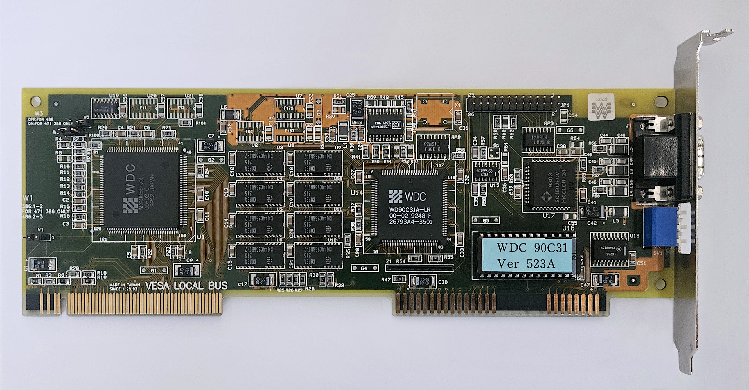
Nifty card. Looks like the WD90C56 is logic to glue an ISA card into a VLB card. https://pdos.csail.mit.edu/6.828/2014/reading … oc/PARADISE.TXT

I've seen some other early VLB cards that did something similar-- https://theretroweb.com/expansioncards/s/tekr … ost-4000-3-plus

But in this case though, the CL-GD5428 chip had built in VLB connectivity, so I wouldn't expect it to need the ASIC glue chip.

Reply 349 of 356, by pshipkov

User metadata
Rank l33t
Rank
l33t

Such bus-interfacing contraptions always catch my eye.
The card you linked is even more weird as there are other ET4000AX VLB based cards that look much simpler. I think the angle with it is to put an ISA IDE and ISA VGA on a single VLB PCB that occupies a single slot instead of two individual ISA cards. Why two ISA chips but not VLB VGA instead (at minimum) - these are questions that tickle.

Yes, the CL-GD5428 card in question is a different case. But it falls in the "weird" VLB bucket with the other two.

retro bits and bytes | DOS media library

Reply 350 of 356, by BitWrangler

User metadata
Rank l33t++
Rank
l33t++

Maybe intended for those single VLB slot 386/486 boards.

Unicorn herding operations are proceeding, but all the totes of hens teeth and barrels of rocking horse poop give them plenty of hiding spots.

Reply 351 of 356, by douglar

User metadata
Rank l33t
Rank
l33t

So .....

  • OP Vic3 is clearly from Opus International
  • OPTi 82C611 chip is clearly OPTi and is called "OPTi VIC" in its driver
  • And so I got to assume that the "OP Vic1" chip that has shown up from time to time is also probably from Opus International, and isn't OPTi
The attachment Op Vic 1.png is no longer available

Reply 352 of 356, by rasz_pl

User metadata
Rank l33t++
Rank
l33t++
douglar wrote on 2026-10-27, 12:22:

It does look like a cheap card, but isn't that a 14Mhz crystal between the MACHSPEED and the 40 pin connector?

Im guilty of posting while falling asleep 🙁

douglar wrote on 2026-10-27, 12:22:

The pinout for that 40 pin connector doesn't look like a memory expansion to me. Looks like an IDE pinout, with pins 19, 22, 24, & 26 going to ground and the I/O traces going to the MACHSPEED chip, not the 5428 like I'd expect for a memory expansion.

You are right. I saw few traces close enough and assumed it was going to ram, looking again vias go to capacitors and resistor on top next to other ram vias going to the VGA chip.

douglar wrote on 2026-10-27, 12:22:

Maybe the MACHSPEED chip attaches both the VGA and IDE to the VLB connector like a glue ASIC to attach two devices to VLB on the same card. It would have to be a little smarter than a couple 74-245 if it was buffering 16 bit ATA into 32bit VLB, but it's hard to know for sure if it tried to do that.

this reminded me of 'Appian Peripheral IF P928' Re: Pre-VESA Proprietary 32-bit Local Buses? supposedly super smart VLB bridge that shipped in whole of one cards and faded to obscurity

https://github.com/raszpl/sigrok-disk FM/MFM/RLL decoder
https://github.com/raszpl/FIC-486-GAC-2-Cache-Module (AT&T Globalyst)
https://github.com/raszpl/386RC-16 ram board
https://github.com/raszpl/Zenith_ZBIOS Zenith Z-386 MFM-300 ZBIOS disassembly

Reply 353 of 356, by douglar

User metadata
Rank l33t
Rank
l33t

Putting my notes on the wiki---

https://www.vogonswiki.com/index.php/VLB_IDE_Controllers

Been doing driver disassembly with Claude.

Interesting notes that I'll need to manually validate:

  • The Micronics MIC491 controller does seem to be software programable
  • The VG4 driver from Promise 20630 only seems set MWDMA-1 (SET FEATURES 21h, DMA levels 7–8); it never sends 22h for MWDMA-2
  • The Flexidriver from Adaptec has a separate code path for the AIC-25PC10 that does seem to include MWDMA-2, but the transfer from the chip to the CPU is still PIO like the Promise 20630 chip

Reply 354 of 356, by douglar

User metadata
Rank l33t
Rank
l33t

It's been a pain to do testing on VLB IDE controllers because the benchmarks are at the mercy of the int13h handler and if you want to try a different driver, you are getting a different int13h. Editing the config sys and rebooting every time you want to change a configuration is painful. Even with boot menus, I can only set up 10 options and I find that limiting. And most of the testing tools are for testing drives, not for testing controllers, so there's all sorts of stuff that I didn't need and were missing some stuff that I wanted to see, like how fast the IDE registers can be read and the response time on simple ATA commands. Then there's the testing errors. Did I forget to shadow the rom? Did I even use the rom? The benchmark doesn't tell me. Do I need to rerun the last 5 tests because I screwed up? Was there a partition alignment issue on that one outlier score? You get the idea. Been hitting roadblocks and time wasting issues for years.

So what to do? How about use some AI coding tools to bypass all that mess ?

I made 3 testing tools in Claude--

  • IDEPROBE.EXE - Tells you all sorts of stuff about your ATA Storage, System and VLB card
  • IDETEST.EXE - Does low level write tests with 32 bit disk access and multi sector transfers if available. Should find unused sectors to work on. Use with caution. Or do file level writes if you don't want to beta test risky things.
  • VLBPIO.EXE - Sets the PIO mode for these VLB IDE controllers on the fly--
    - ADD2 DW729
    - Appian ADI/2
    - Adaptec AIC-25PC10 (Untested)
    - Atronics IDE-2015PL
    - CMD PCI0640B
    - Holtek HT6560A & HT6560B
    - Lion 3+
    - OPTI 82C611 & 82C611A
    - Promise PDC-20230c
    - Promise PDC-20630
    - QDI Vision 6500
    - QDI Vision 6580
    - SIS 85C407 aka MIC491 (Untested)
    - SIS 83C601 & SIS 83C611
    - UMC UM8672F
    - VIA VT83C461 (Still working on getting the best performance)
    - VIA VT82C496G (Untested)
    - Winbond W83759AF (Still working on getting the best performance)

Now the only major impediment to doing lots of tests is swapping cards and drives.

Does anyone have working AIC-25PC10, SIS 85C407, MIC491, or VIA VT82C496G cards that would be willing to try out the tools?

The attachment VLBPIO.zip is no longer available

I'll post my benchmark scores next week

Reply 355 of 356, by Dorunkāku

User metadata
Rank Member
Rank
Member

The SIS 85C407 does not belong in that list. It is a realtime clock with SRAM.

I really enjoy deep dives like this and am looking forward to the benchmark scores.

Reply 356 of 356, by douglar

User metadata
Rank l33t
Rank
l33t
Dorunkāku wrote on Yesterday, 21:25:

The SIS 85C407 does not belong in that list. It is a realtime clock with SRAM.

I really enjoy deep dives like this and am looking forward to the benchmark scores.

This post seems to suggest that it is a programmable ISA buffer, which is essentially a primitive PATA bridge. Were they mistaken? “MIC491 - SiS 85C407 ISA bus buffer. “

Re: 80486 BIOS image collection

I found a BIOS that seemed to use programmable registers to change the speed for the IDE devices from Normal, Fast and Turbo and used that info.

I have a card with a MIC491 chip, but the IDE controller didn’t show up on my test system. Maybe I need to try on a Micronics motherboard or a SiS chipset.