VOGONS


First post, by Fallaxia

User metadata
Rank Newbie
Rank
Newbie

Hi Folks,

I would like to upgrade my TI5VG+ mainboard to 1MB or 2 MB of L2 Cache to be able to use more cached RAM in WB/WT mode.
Currently the mainboard has 512 KB of L2 Cache using an UMC UM61L6464AF-5

I plan on upgrading it with a LP61L64128F-4 or LP61L64128F-4/HA

https://www.utsource.net/de/itm/p/6917515.html

LP61L64128F-4.webp

Not sure if there are any 2 MB chips out there or better alternatives with 1Mb or 2 MB at all.
Can anyone recommend some SRAM / cache chip options?

Reply 1 of 4, by rasz_pl

User metadata
Rank l33t
Rank
l33t

what about L2 Tag RAM?
how much difference does the L2 give? have you benchmarked anything with L2 turned off?
what CPU? if K6-2+/3 then there wont be any difference

https://github.com/raszpl/FIC-486-GAC-2-Cache-Module for AT&T Globalyst
https://github.com/raszpl/386RC-16 memory board
https://github.com/raszpl/440BX Reference Design adapted to Kicad
https://github.com/raszpl/Zenith_ZBIOS MFM-300 Monitor

Reply 2 of 4, by majestyk

User metadata
Rank Oldbie
Rank
Oldbie

I haven´t seen 2 MB chips in a QFP-128 package so far.
Given VIA´s MVP3 chipset, for 2MB L2 cache you would need a 32-pin TAG RAM (512K), if there are landings for a 28-pin TAG chip on your mainboard and / or only one position for a QFP-128 L2 chip - forget about 2MB.

For 1 MB L2 cache just replace the existing chip and adapt the 0-ohm resistors accordingly.

Reply 3 of 4, by Fallaxia

User metadata
Rank Newbie
Rank
Newbie

@rasz_pl
I am currently trying to get a comprehensive (true) performance benchmark of various CPUs. Starting with early Pentium 1 over to Pentium MMX, Cyrix 6x86 / MII, to RiseMp6, WinChip 1 / 2 to AMD Geode and AMD K6-2 and K6-3+

To do that I use a current Linux Kernel together with AntiX / gentoo Linux while the Kernel is optimized for the respective CPU installed. It then runs I/O based, memory, network etc. tests which can be compared with the other CPUs to get a comprehensive overview of the true potential of these CPUs (under optimal enviroment conditions / optimized code and feature usage.

However, this requires a good amount of RAM. 256 MB at the very minimum, better 512 MB to avoid swapping, which would invalidate any I/O based results.

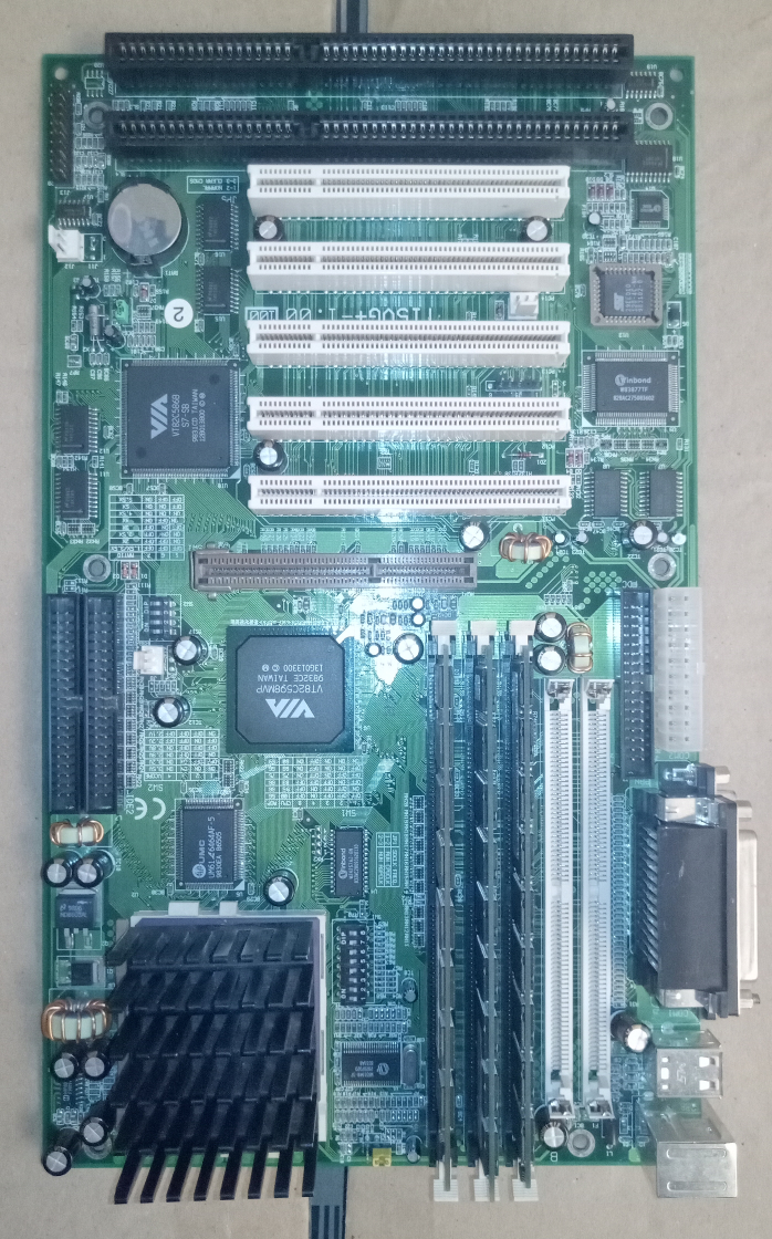
That´s why I try to equip a SS7 mainboard with ideally 2 MB of L2 cache.

I have several boards available, like the already mentioned Shuttle Ti5VG+ to the GA-5AA and the ASUS P5A, Gigabyte GA-5AX to name a few.
Unfortunately most come with only 512KB of L2 cache. (I sold my EP-MVP3G5 too early)

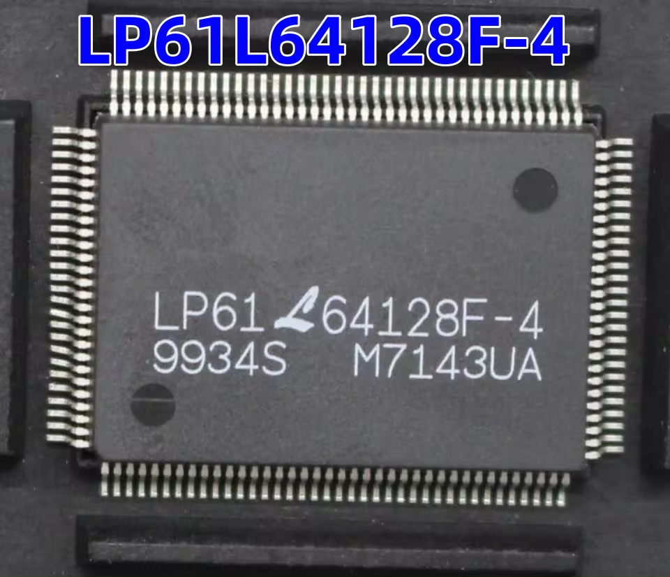
I took some photos of the Ti5VG+ and it seems it has a TAG ram of 512K as well as two QFP128 pads, one on the component side and one on the back, if I am not mistaken, see photo.

TI5VG+ with 512K SRAM and TAG 512K

TI5VG_02.jpg

Rear view with PCB pad for additional SRAM QFP128 ?
TI5VG_01.jpg
This SRAM / TAG is currently on the board
TI5VG_03.jpg

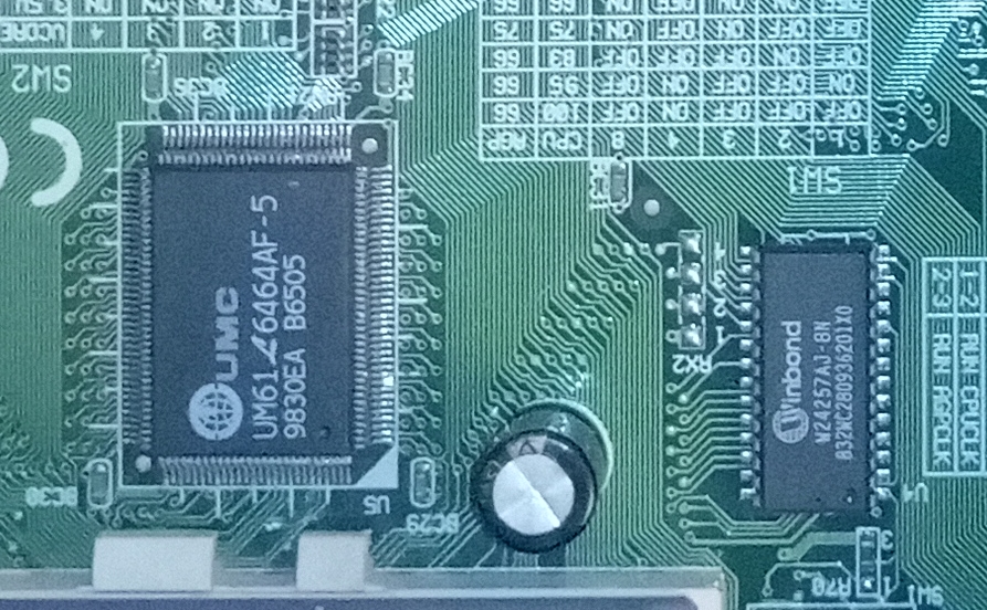
Does anyone know if the rear pad is a "real" pad and if it´s possible to solder two 8Mbit SRAM chips to it to replace the current 4 Mbit one?

Reply 4 of 4, by majestyk

User metadata
Rank Oldbie
Rank
Oldbie

Wishful thinking, you should have kept your MVP3-G5 😀

The TAG chip is 256K, 28 pin [32K x 8] - don´t bother about 2MB cache.

_All_ you can do is add a second 512K cache chip on the flip side or maybe replace the existing 512K by a 1M chip. The 2-chip solution is superior because L2 interleave is possible.

The limits for cacheable RAM area are 256 MB (write through) or 128 MB (write back) with this setup. Many MVP3 boards don´t offer WB L2 due to BIOS limitations or they switch between WB / WT automatically depending on RAM size.