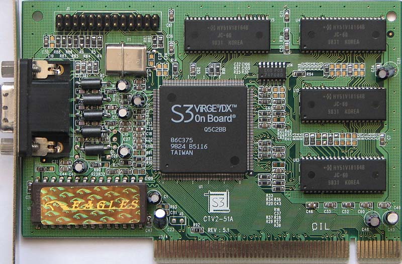
As I like examining hardware with interesting design, I stumbled across Virge DX cards with 8MB of RAM soldered onto them. One of those cards is owned by forum user Disruptor, another of them is owned by Vlask, and exhibited in the VGA museum. The memory chips on Disruptor's cards are four chips LGS GM71C18163C. The memory chips on Vlask's card are four chips Hyundai HY51V18164B. The design of both cards is quite similar, and rather curious. The memory chips are 1M x 16 in both cases, organized as 1024 rows of 1024 columns of 16 bits each. Simple maths shows you that each of the chip contain 2MB, so all four of these chips contain 8MB total. So there are Virge DX cards with 8MB RAM. Case closed.
No, not so fast! Case reopened! The conclusion of the first paragraph is technically correct, but if that would be the whole story, I wouldn't bother writing a VOGONs post about this kind of card. Let's start with the observation that the VESA BIOS of Disruptor's card only reports 4MB of RAM. The Virge DX (86c375) is basically just a performance-enhanced classic Virge (86c325), and the Virge DX is fully pin compatible to the classic Virge in PCI mode. You can find the full data sheet for the classic Virge chip. I'm not going into rambling about the meaning of "full" is this context, but it most likely is the most complete data sheet for the Virge chip ever published, so I'm going to call it "full". This data sheet explains the memory organization of the Virge: You can have either one or two banks of 2MB each, organized as 256K x 64. You can use two banks of memory in PCI mode only, but this thread is about the Virge DX and Virge GX, which don't support VL mode any more, so let's not bother about it. The adressing scheme is 9 column bits and 9 row bits. The multiplexing between row and column chips is performed inside the Virge chip, so there are just 9 memory address lines (MA0-MA8). You can't address the 1M x 16 chips, which need 10 memory address bits using this scheme.
So basically, one of two cases are possibly: Either I was wrong by claiming that "the Virge DX memory interface is identical to the Virge memory interface", and the Virge DX in fact does support 10 memory address lines (e.g. by optionally repurposing the second "bank enable" pin as a tenth address pin, to support one bank of 8MB). Or the card contains some glue logic to address the bigger chips without the Virge chip knowing about it. The actual situation is: This kind of card contains some glue logic. The card by Vlask I linked has the 74F08 chip clearly visible near the top left corner. Disruptor's card has a SMD logic chip (most likely also a 74F08) below the OTP ROM chip, which is soldered (not in a socket) to the card. That's why I didn't bother taking and posting a picture of Disruptor's card - the one interesting piece on that card is not visible on that card, but clearly visible on Vlask's card.
The card works like this: MA9 (the tenth address pin of the memory chips) is connected to /RAS1 (the second bank enable signal). So MA9 is high the whole cycle when the Virge (DX) tries to address the "first" bank, whereas MA9 is low the whole cycle when the Virge (DX) tries to address the "second" bank. The /RAS1 pin does not change between the row and column addressing phase, so if the Virge chip tries to access the first bank, it gets into the second half of rows and the second half of columns. When the Virge chip tries to access the second bank (it activates, i.e. lowers, /RAS1), it gets into the first half of rows and the first half of columns. At no time, a low column from a high row, or a high column from a low row is addressed. This degrades the usable address range of the chips that contain 2MB per chip to 1MB per chip. And four of those chips make 4MB accessible video RAM. Case closed for good.. If you are curious about the 74F08 chip I mentioned: The Virge chip has a pin to activate the first bank (/RAS0) and a different pin to activate the second bank (/RAS1). But the card only contains one bank of chips that needs to be activated on any memory cycle. And that's where the 74F08 kicks in: It's a "quad AND gate". Let's first forget about the "quad" part: Only one of the four AND gates is used. Now, you need to consider that the bank activation signals are active low. So the signal is high if the bank is not active. When you combine a signal that is high if bank 0 is not active with a signal that is high if bank 1 is not active using an AND gate, you get a signal that is high if bank 0 is not active AND bank 1 is not active, i.e. neither bank is active. So the signal is low is either bank is active, which is exactly what we need to feed into the one bank of RAM chips to activate it (by a signal that is low to activate the chips).
So why would you waste half of the memory? As the cards look like generic OEM cards, most likely are cost optimized, and the conclusion is that cards containing 4 chips of 2MB (1M x 16) were cheaper to build than cards containing 8 chips of 512KB (256K x 16), although you need to supply twice as much memory. This can either be due to 256K getting "uncommon" and more expensive, or due to the PCB being smaller with only 4 memory chips. Having only 4 memory chips also simplifies routing the address and data lines. There is a strong indication that actually routing is the key point: Take a look at the back side of Vlask's card. You find that the back side is mainly ground interrupted by some think traces which are most likely 5V. This a strong indication that this card does not have internal power planes! So using only a single bank of memory enables the card manufacturer to use a 2-layer PCB instead of a 4-layer PCB. A PCB with no internal layers is way cheaper to build than a PCB with internal layers (which is kind-of two two-layer PCBs precisely glued together). So the explanation for that card is: The additional cost for 8MB instead of 4MB of RAM is more than compensate by savings from being able to use a 2-layer PCB.
TL;DR: There are Virge DX cards in the wild that contain 8MB of memory. The Virge DX chip is unable to address 8MB of memory. Some clever circuits on the card pack 2 banks of 2MB into the 8MB, not using half of the chips using only 50% of the memory in each individual chip. The reason for those card to exist is most likely due to manufacturing costs.
EDIT: clarified statement in the TL;DR.


