On a mobo I used to have there was a non functional 83 mhz option that was asynchronous I believe the reason it didn’t work was the chipset or mobo wasn’t able to go async. I suspect your no boot option may be that. Mine also would not boot. My understanding was it was because of the rest of the mobo, not the chip.
On a mobo I used to have there was a non functional 83 mhz option that was asynchronous I believe the reason it didn’t work was the chipset or mobo wasn’t able to go async. I suspect your no boot option may be that. Mine also would not boot. My understanding was it was because of the rest of the mobo, not the chip.
You might be right but... according to my research, "HiZ" means "floating", so I'm inclined to believe that it actually doesn't produce any signal (I may be wrong).
Keep in mind this circuit was used by "PC-Chips" for their mainboards, so you´re supposed to expect some fake information... 😉
Yes, but... is CYPRESS in any way related to PC-Chips and its shenanigans? I wasn't aware of that.
To be fair PC-Chips/Hsing Tech Enterprise made some good boards. That doesn't compensate all the damage they did with their defective and fake cache boards...
FWIW this board is working rather well so far. The only one with the TX chipset that is fully compatible with the R9250 DVI output (that I could find) and.. I appreciate the 33MHz bus option 🐢
Hopefully I'm not bringing this too far out of the grave...
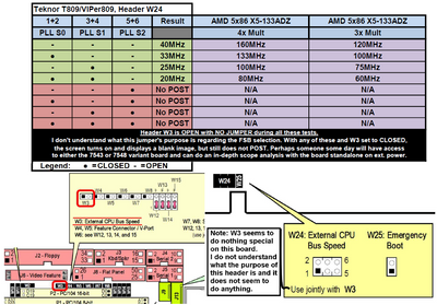
I have a Socket 1 SBC here from Teknor, a VIPer809 with a Cirrus 7548 VGA chipset. PLL is a Cypress CY2291F. Datasheet and manuals attached.
I've figured out that pins 14/15/17 are S0/S1/S2 respectively and coincide with header W24 pins 2/4/6 on this board.
I've laid out the various frequencies I've been able to get out of it in the table below.
Testing graph showing what I've already figured out
File license
Public domain
There's also a header W3 which is mentioned in the quick reference and in the manual, but it only ever appears to be left open. This is rather weird. if I apply a jumper to it I get a blank screen if it makes it far enough through to initialize the graphics chip, but no POST. All of these tests were done with an AMD 5x86 X5-133ADZ which I have successfully tested in the past (like 15 years in the past) to do the sweet spot of 160MHz. I was hoping this board would allow me to try and go further and see if I have a golden chip capable of 180-200MHz, but I guess not at this moment.
The PLL datasheet says there's 8 possible combinations for frequencies which I do not understand if there's only three possible pins to jumper, and so far I can only get two.
Maximum that the PLL can do is either 66.6MHz or 90MHz depending on if it's provided with 3.3v or 5V in respectively, and if an external crystal is used for the reference clock, which in this case it is, so this is likely being fed 5v.
Pin 6 of W24 is an unknown frequency going to/from the PLL. I don't have a scope handy to run the board externally and check what it's outputting, either, which is a bit of an issue. I'm planning on getting my hands on a cheap scope later on down the line but for now I wanted to drop this information in here lest it help someone else down the line with one of these PLLs on this board or any other.