VOGONS


Clock generators on Socket 7 and older motherboards

Topic actions

Reply 80 of 96, by Sphere478

User metadata
Rank l33t++
Rank
l33t++

On a mobo I used to have there was a non functional 83 mhz option that was asynchronous I believe the reason it didn’t work was the chipset or mobo wasn’t able to go async. I suspect your no boot option may be that. Mine also would not boot. My understanding was it was because of the rest of the mobo, not the chip.

Sphere's PCB projects.
-
Sphere’s socket 5/7 cpu collection.
-
SUCCESSFUL K6-2+ to K6-3+ Full Cache Enable Mod
-
Tyan S1564S to S1564D single to dual processor conversion (also s1563 and s1562)

Reply 81 of 96, by tauro

User metadata
Rank Member
Rank
Member
Sphere478 wrote on 2023-09-01, 03:53:

On a mobo I used to have there was a non functional 83 mhz option that was asynchronous I believe the reason it didn’t work was the chipset or mobo wasn’t able to go async. I suspect your no boot option may be that. Mine also would not boot. My understanding was it was because of the rest of the mobo, not the chip.

You might be right but... according to my research, "HiZ" means "floating", so I'm inclined to believe that it actually doesn't produce any signal (I may be wrong).

Reply 82 of 96, by majestyk

User metadata
Rank Oldbie
Rank
Oldbie

Hi-Z should mean "high-impedance", while all the outputs of the clock generator need to be low impedance during regular operation.

Keep in mind this circuit was used by "PC-Chips" for their mainboards, so you´re supposed to expect some fake information... 😉

Reply 83 of 96, by tauro

User metadata
Rank Member
Rank
Member
majestyk wrote on 2023-09-01, 05:13:

Hi-Z should mean "high-impedance", while all the outputs of the clock generator need to be low impedance during regular operation.

So if I understand correctly, this would mean that it effectively doesn't produce any useful signal (no 83MHz).

majestyk wrote on 2023-09-01, 05:13:

Keep in mind this circuit was used by "PC-Chips" for their mainboards, so you´re supposed to expect some fake information... 😉

Yes, but... is CYPRESS in any way related to PC-Chips and its shenanigans? I wasn't aware of that.

To be fair PC-Chips/Hsing Tech Enterprise made some good boards. That doesn't compensate all the damage they did with their defective and fake cache boards...

FWIW this board is working rather well so far. The only one with the TX chipset that is fully compatible with the R9250 DVI output (that I could find) and.. I appreciate the 33MHz bus option 🐢

Reply 84 of 96, by majestyk

User metadata
Rank Oldbie
Rank
Oldbie

Just joking here - Cypress is / was a renowned company.

Reply 86 of 96, by Sudos

User metadata
Rank Newbie
Rank
Newbie

Hopefully I'm not bringing this too far out of the grave...
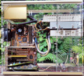
I have a Socket 1 SBC here from Teknor, a VIPer809 with a Cirrus 7548 VGA chipset. PLL is a Cypress CY2291F. Datasheet and manuals attached.
I've figured out that pins 14/15/17 are S0/S1/S2 respectively and coincide with header W24 pins 2/4/6 on this board.
I've laid out the various frequencies I've been able to get out of it in the table below.

The attachment W24Testing.png is no longer available

There's also a header W3 which is mentioned in the quick reference and in the manual, but it only ever appears to be left open. This is rather weird. if I apply a jumper to it I get a blank screen if it makes it far enough through to initialize the graphics chip, but no POST. All of these tests were done with an AMD 5x86 X5-133ADZ which I have successfully tested in the past (like 15 years in the past) to do the sweet spot of 160MHz. I was hoping this board would allow me to try and go further and see if I have a golden chip capable of 180-200MHz, but I guess not at this moment.

The PLL datasheet says there's 8 possible combinations for frequencies which I do not understand if there's only three possible pins to jumper, and so far I can only get two.
Maximum that the PLL can do is either 66.6MHz or 90MHz depending on if it's provided with 3.3v or 5V in respectively, and if an external crystal is used for the reference clock, which in this case it is, so this is likely being fed 5v.

Pin 6 of W24 is an unknown frequency going to/from the PLL. I don't have a scope handy to run the board externally and check what it's outputting, either, which is a bit of an issue. I'm planning on getting my hands on a cheap scope later on down the line but for now I wanted to drop this information in here lest it help someone else down the line with one of these PLLs on this board or any other.

8ips6a-2.png
qxkaxq-2.png

Reply 87 of 96, by Mr.Hunt

User metadata
Rank Newbie
Rank
Newbie
lazibayer wrote on 2017-09-21, 19:20:

Stolen from

Kamerat wrote:

The Gigabyte GA-6EM have a clock generator capable of 33MHz FSB, the PLL52C66-05. You might have to modify the board to get access to the lowest clocks.

It goes from 33MHz all the way up to 100MHz.

Hello! Could you please attach pdf datasheet for this clocker ? I have super socket 7 GA-5AA motherboard and want to change clocker for more lower. For me it would be great from 33 to 100. But i cannot find what i can use. pinouts all of clocker are not comparable 🙁

Reply 88 of 96, by Recycled_Box

User metadata
Rank Newbie
Rank
Newbie

I'd like to bump the thread with the question; can there be no universal guide on translating these tables into the jumpers on the board you happen to have in your collection?

Because from what I can see there are no universal rules to doing this other than "try it and see" but I'm afraid of damaging some hardware I own by moving some jumpers around that I shouldn't be moving.

Reply 89 of 96, by PARKE

User metadata
Rank Oldbie
Rank
Oldbie

The point of this thread is to provide info on how to interprete the various ways how motherboard manufacturers implemented multi clock jumper configurations. There was no standard for that. I don't think that you can damage hardware by trying out different multipliers or, for that matter, different fsb settings. Just do not experiment with voltage settings, those can really hurt.
Here you find an article that gives some insight in the basis of multi clock implementation:
http://pchardwarelinks.com/cpuspeed.htm

Reply 91 of 96, by Lostdotfish

User metadata
Rank Member
Rank
Member

TMC/MyComp/MyNix/Megastar - TI5TT (VER. 1.1)
https://theretroweb.com/motherboards/s/tmc-my … -ti5tt-ver.-1.1

ICS9148F-25

The attachment Screenshot 2025-03-05 152247.png is no longer available

Interestingly, my board only has half the DIP switches populated

The attachment Screenshot 2025-03-05 152520.png is no longer available

I've traced the switches with a meter and 2 is connected to FS0. Unpopulated 6 is connected to FS1 and unpopulated 7 is connected to FS2. This agrees with the truth table above, FS1 and FS2 will always be high as they have no switch to ground them. FS0 is used to toggle between 60 and 66.8 MHz clock.

I've ordered an 8 switch DIP to see if I can open up the other clock options on the table above. 75MHz operation is quoted in the board manual but it will be interesting to see if 83.3MHz and 55MHz also work.

I assume this means the rest of the switches (1, 2, 4, 5 and 8.) are setting the multiplier? Is the multiplier also on this ICS IC? Or do those switches head elsewhere?

Reply 92 of 96, by myne

User metadata
Rank Oldbie
Rank
Oldbie
Sudos wrote on 2024-01-11, 08:04:

The PLL datasheet says there's 8 possible combinations for frequencies which I do not understand if there's only three possible pins to jumper, and so far I can only get two.

000
001
010
011
100
101
110
111

Welcome to binary 😀

I built:
Convert old ASUS ASC boardviews to KICAD PCB!
Re: A comprehensive guide to install and play MechWarrior 2 on new versions on Windows.
Dos+Windows 3.11+tcp+vbe_svga auto-install iso template
Script to backup Win9x\ME drivers from a working install
Re: The thing no one asked for: KICAD 440bx reference schematic

Reply 93 of 96, by Sphere478

User metadata
Rank l33t++
Rank
l33t++

The multipler goes to one to three pins on the cpu which will be one to three of four possible pins.

Bf0,bf1,bf2 (amd/cyrix),bf2 (intel)

These pull low at about 25-500 ohm
And pull high at about 300-2100 ohm depending on mfg

Your resistor combo should see the pull high resistance much higher than the pull low resistance

It’s a voltage divider meant to over power the pull high resistor

Sphere's PCB projects.
-
Sphere’s socket 5/7 cpu collection.
-
SUCCESSFUL K6-2+ to K6-3+ Full Cache Enable Mod
-
Tyan S1564S to S1564D single to dual processor conversion (also s1563 and s1562)

Reply 94 of 96, by Lostdotfish

User metadata
Rank Member
Rank
Member
Lostdotfish wrote on 2025-03-05, 15:32:
TMC/MyComp/MyNix/Megastar - TI5TT (VER. 1.1) https://theretroweb.com/motherboards/s/tmc-my … -ti5tt-ver.-1.1 […]
Show full quote

TMC/MyComp/MyNix/Megastar - TI5TT (VER. 1.1)
https://theretroweb.com/motherboards/s/tmc-my … -ti5tt-ver.-1.1

ICS9148F-25

The attachment Screenshot 2025-03-05 152247.png is no longer available

Interestingly, my board only has half the DIP switches populated

The attachment Screenshot 2025-03-05 152520.png is no longer available

I've traced the switches with a meter and 2 is connected to FS0. Unpopulated 6 is connected to FS1 and unpopulated 7 is connected to FS2. This agrees with the truth table above, FS1 and FS2 will always be high as they have no switch to ground them. FS0 is used to toggle between 60 and 66.8 MHz clock.

I've ordered an 8 switch DIP to see if I can open up the other clock options on the table above. 75MHz operation is quoted in the board manual but it will be interesting to see if 83.3MHz and 55MHz also work.

I assume this means the rest of the switches (1, 2, 4, 5 and 8.) are setting the multiplier? Is the multiplier also on this ICS IC? Or do those switches head elsewhere?

The attachment Screenshot 2025-03-07 125153.png is no longer available

75MHz bus unlocked

The attachment Screenshot 2025-03-07 125207.png is no longer available

83.3MHz bus unlocked

The attachment Screenshot 2025-03-07 132107.png is no longer available

K6-2 400 happily chugging along at 6x75

Reply 95 of 96, by myne

User metadata
Rank Oldbie
Rank
Oldbie

Not too long, and you'll be looking through alldatasheet for pin compatible replacements.

It's p2+ era, but here's a bunch I can add to the thread.
Should paste into excel and make sense

ICS						hublink					
xx Chip format CPU# CPU volts SDRAM# PCI# 66mhz? Jumpers minMhz Maxmhz Serial VID max clocks Other/notes
ICS9250-08 56ssop 3 2.5 17 7 0 4 66 133 150
ICS9250-10 56ssop 3 2.5 9 8 2 2 66 100 133
ICS9250-12 56ssop 4 2.5 0 8 4 2 100 133 NA 2xcpu/2. For rambus systems
ICS9250-18 56ssop 3 2.5 17 7 0 4 66 150 166
ICS9250-23 56ssop 2 2.5 13 8 2 5 66 166 same as jumpers
ICS9250-27 56ssop 3 2.5 9 7 3 3 66 133 same as jumpers
ICS9250-50 56ssop 2 2.5 13 8 3 5 66 133 undocumented
ICS9250-16 56ssop 3 2.5 9 8 0 3 66 133 150
ICS9212-13 - - - -- - - - - - rambus
ICS9250-28 56ssop 2 2.5 13 2 3 3 66 133 same as jumpers
ICS9150F-04 56ssop 5 16

I built:
Convert old ASUS ASC boardviews to KICAD PCB!
Re: A comprehensive guide to install and play MechWarrior 2 on new versions on Windows.
Dos+Windows 3.11+tcp+vbe_svga auto-install iso template
Script to backup Win9x\ME drivers from a working install
Re: The thing no one asked for: KICAD 440bx reference schematic

Reply 96 of 96, by Lostdotfish

User metadata
Rank Member
Rank
Member

55MHz bus is also working.

My K6-2 400 AFK craps out if I set 83.3MHz bus but my 450AFX is happy

The attachment Screenshot 2025-03-07 154333.png is no longer available

Who needs Super Socket 7...