VOGONS


Reply 200 of 1193, by feipoa

User metadata
Rank l33t++
Rank
l33t++
Aerion wrote on 2021-06-17, 07:25:

@feipoa:
Sorry that I have not reported here more. Unfortunately I have other PCB projects and too little time.
I will continue this as soon as possible, although I do not own a CPU of this type myself. So I can not test this.

Glad to hear you are still alive. I thought maybe COVID got ya dead.

Never enough time. And there will only be less as time goes on.

I can test it if you ship the PCB and components. Or if the components are also available on digikey.ca, mouser,ca, or newark.ca, I can order them myself.

Two months ago, thinking you might get a PCB sample ready, arrangements were made to have a dozen of these CPUs reserved. So if you need one for testing, they are available.

Plan your life wisely, you'll be dead before you know it.

Reply 201 of 1193, by Anonymous Coward

User metadata
Rank l33t
Rank
l33t

Somebody send that man a CPU, ASAP.

"Will the highways on the internets become more few?" -Gee Dubya
V'Ger XT|Upgraded AT|Ultimate 386|Super VL/EISA 486|SMP VL/EISA Pentium

Reply 202 of 1193, by Aerion

User metadata
Rank Newbie
Rank
Newbie

Fortunately, COVID did not affect me and my family is healthy. Several of my colleagues have fallen ill. Since I'm in the home office, I have to do a lot of development work. Worse than at work...
I hope to resume PCB design soon.

Niemand ist nutzlos, er kann immer noch als schlechtes Beispiel dienen...

Reply 203 of 1193, by Blavius

User metadata
Rank Newbie
Rank
Newbie

Hi, is there any update on this? I would love to have one! I've been trawling local sites for a PGA132 clock doubling DLC to no avail, but I have a PGA168 lying around I could use with this interposer. I was thinking about making one myself, but as I have no experience with Eagle, nor the high frequency design principles, it's pretty daunting.

Reply 206 of 1193, by Blavius

User metadata
Rank Newbie
Rank
Newbie

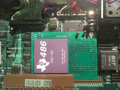
I had a 168 pin TI486 SXL-40 lying around that I bought a few years ago, thinking it was a 132 pin. I'm sure I wasn't the only one that fell for this. Always wanted to see if it worked, and I followed this thread for a bit. In the end, I rolled up my sleeves, got into KiCAD, took CB88's latest draft and adapted it to my needs.

IMG_3846.JPG
Filename
IMG_3846.JPG
File size
85.49 KiB
Views
1049 views
File license
CC-BY-4.0

Before I start, let's get a few things out of the way:
-This is my second PCB ever; I am confident that to a professional it looks like a toddlers doodle
-I selfishly made this to fit my computer (IBM P70 luggable), it may not fit yours - this is not an universal interposer
-I'm running with a 20MHz clock, doubled to 40MHz. The trace length is such, that for 40/80MHz it should still fall in the 2.5% skew allowed by JEDEC. So, it could work at those frequencies, but I have no way to test this
-I'm still having issues getting the cache working. The board doesn't have any coherency circuits, something I regret now.

Design and build
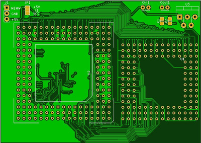
In this thread, the envisioned end product would be a pcb roughly the size of the processor, with pins at the bottom and a socket at the top. This would require a smd 168 sockets, and a smd 132pin array. Despite extensive searching, I did not find these components. I did however have a though-hole 168pin socket (for 486s) lying around. I reckoned the only way to have two though hole arrays would be to put them side by side.
This is of course not ideal - wire lenght increases - but it was the only way I saw this becoming a practical reality. I updated the circuit of CB88 (who left a few pins unconnected) and added in the MIC29152 regulator discussed in this thread. The real work was laying out the tracks. What you see here is my third attempt; earlier versions always drowned half-way because of too large traces or orientating the sockets in the wrong way. The traces are now the thinnest allowed by JLCPCB, and even then it barely fits here and there.

pcb.jpg
Filename
pcb.jpg
File size
265.07 KiB
Views
1049 views
File license
CC-BY-4.0

The PCB does not have many options. The power regulator puts out 3.5V. This is fixed, but can be altered by changing out R1. There is a header for a 5v fan and a connection to the MEMW pin. Also, there is a solderjumper that allows to set pin J1 to 5V or vcc (3.5V). Only make this 5V for the SXL-G40 and SXL2-G50, all other SXL processors need vcc (3.5V).

The 132 pin side is just holes. I bought 0.5mm 24AWG wire. I used a space 132 pin socket placed at the right distance to accept the wire, solder it, cut it off. Repeat, 131x. The result is a pin array that is surprisingly rigid, not much worse than an actual processor.

Testing
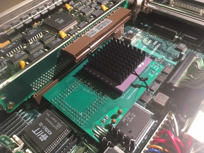
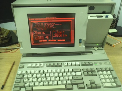
My system (IBM PS/2 P70) started normally with the interposer. I used the cyrix.exe utility to double the clock (-cd), which took it to 40MHz in Norton sysinfo. I did add a little heatsink, as the processor got quite toasty (not burning my fingers though).

IMG_3847.JPG
Filename
IMG_3847.JPG
File size
96.51 KiB
Views
1049 views
File license
CC-BY-4.0
IMG_3848.JPG
Filename
IMG_3848.JPG
File size
70.62 KiB
Views
1049 views
File license
CC-BY-4.0

I've been less lucky with the cache though. Getting the cache working on the 486DLC that was in there originally was already a headache - I got it kinda working with flush and defining an exepted space. But for the 486SXL-40 none of this works. Flush (-f) or Barb (-b) don't do anything, doom isn't faster and the cache doesn't end up in cachecheck. As soon as I exept a portion of the memory the system becomes unstable. I don't think this is a fault of the interposer, more of compatibility issues between my (1989-) computer and the processor.
In any case- suggestions for how to get that working? I have seen mentions of some simple circuit that is needed to get cache coherency with Flush, but couldn't find anything on it. Can anyone point me to where I can find something on that?

Attachments

Reply 207 of 1193, by feipoa

User metadata
Rank l33t++
Rank
l33t++

Nice work. To make the sockets on top of each other, I'm fairly confident you'd need 4 or 6 layers. From what I can tell, your design is 2-layer?

You can still find PGA-132 and PGA-168 sockets NOS, usually on eBay or via some electronic warehouses throughout the US or China. I know I have a bin with some. But you can also use single row machine pins to form up the sockets, like I did with my first wire board prototype.

Any reason you decided not to include the through holes for the trimmer to make this unit adjustable?

As for why you are having issues with cache coherency, I don't know. The MEMW circuit can be found in the TI486SXL databook, which unfortunately, is too large for me to attach here. I was pretty sure there was a link to it in this thread though, is there not? If nothing turns up, I can PDF the few pages of interest in the next few days. I'm trying to get my home's foundation put back together before the rain comes, so no time at the moment. I'm replacing the perimeter drains and sewer pipes by hand with paver surrounding the home. It is considerably exhausting.

If you have a spare board, populated, or unpopulated, that you'd like to mail, I can test it out further.

Plan your life wisely, you'll be dead before you know it.

Reply 208 of 1193, by Sphere478

User metadata
Rank l33t++
Rank
l33t++

Stares in: “I don’t need another project but this is cool” must resist…

Sphere's PCB projects.
-
Sphere’s socket 5/7 cpu collection.
-
SUCCESSFUL K6-2+ to K6-3+ Full Cache Enable Mod
-
Tyan S1564S to S1564D single to dual processor conversion (also s1563 and s1562)

Reply 209 of 1193, by Sphere478

User metadata
Rank l33t++
Rank
l33t++

If I am understanding this right, you are trying to adapt a 486 into a smaller 386 socket? With voltage interposer capability. Tl:dr

I haven’t looked much into the pinout of 386 sockets, but I know they are a smaller footprint and I believe not pin compatible on the rows that do overlap. So a straight through interposer isn’t going to work.

A surface mount style design may be possible.

But off setting it is certainly easier to assemble. So the designs I see in pics look pretty practical.

My only other idea would be using pin headers to make a stack to divorce two pcbs this would be pretty compact and not too hard to assemble which would be a huge help. Similar to my idea here:

Re: Socket 5/7/SS7 VOLTAGE Interposer.

Also:

Re: Socket 370 Tweaker been looking into a surface mount style style setup for this

Socket 1/2/3 Voltage Interposer Tweaker (Alpha)
Here is some info I gathered on socket 1/2/3 tweaks.

Sphere's PCB projects.
-
Sphere’s socket 5/7 cpu collection.
-
SUCCESSFUL K6-2+ to K6-3+ Full Cache Enable Mod
-
Tyan S1564S to S1564D single to dual processor conversion (also s1563 and s1562)

Reply 210 of 1193, by Blavius

User metadata
Rank Newbie
Rank
Newbie
feipoa wrote on 2022-09-09, 21:37:

Nice work. To make the sockets on top of each other, I'm fairly confident you'd need 4 or 6 layers. From what I can tell, your design is 2-layer?

Cheap as I am, I used 2 layer. For a stack you will undoubtedly need four.

Any reason you decided not to include the through holes for the trimmer to make this unit adjustable?

I wasn't planning on overclocking, but there was plenty of room to integrate them. That is an oversight.

As for why you are having issues with cache coherency, I don't know. The MEMW circuit can be found in the TI486SXL databook, which unfortunately, is too large for me to attach here. I was pretty sure there was a link to it in this thread though, is there not? If nothing turns up, I can PDF the few pages of interest in the next few days. I'm trying to get my home's foundation put back together before the rain comes, so no time at the moment. I'm replacing the perimeter drains and sewer pipes by hand with paver surrounding the home. It is considerably exhausting.

I have a copy of the databook, and for the 168 pin version the MEMW circuit is built into the chip. Only thing to do is connect the MEMW pin to the ISA MEMW. Only thing is; I have a MCA system which doesnt have a MEMW pin. Maybe I should ask TexElec or something...

Screenshot 2022-09-10 073152.jpg
Filename
Screenshot 2022-09-10 073152.jpg
File size
41.88 KiB
Views
1011 views
File license
CC-BY-4.0

Alternatively I could BARB, but unless my board supports 'hidden refresh' (I'm guessing not) the cache would be invalidated so often as not to be useful.

Screenshot 2022-09-10 073744.jpg
Filename
Screenshot 2022-09-10 073744.jpg
File size
42.12 KiB
Views
1011 views
File license
CC-BY-4.0

If you have a spare board, populated, or unpopulated, that you'd like to mail, I can test it out further.

I only populated one board and have four empty spares, so if you dont mind to hunt down the components I'd be happy to send you one. Just give me a DM.

Here's the KiCad project btw:

Filename
CPUInterposer386-486.zip
File size
3.29 MiB
Downloads
42 downloads
File license
CC-BY-4.0

Reply 211 of 1193, by Blavius

User metadata
Rank Newbie
Rank
Newbie
Sphere478 wrote on 2022-09-09, 22:42:

If I am understanding this right, you are trying to adapt a 486 into a smaller 386 socket? With voltage interposer capability. Tl:dr

It looks like it, but no; this is meant for a particular processor which is not a true 486, but uses the same socket. The 'normal' version of the TI486SXL is meant as a drop-in replacement for a 386 and has 132 pins. For some reason a version of the chip was put in a 168 pin package, which is identical to the 132 pin, but the position of the pins is completely different. This interposer translates that back to 132 pin. And supplies the needed lower voltage.

My only other idea would be using pin headers to make a stack to divorce two pcbs this would be pretty compact and not too hard […]
Show full quote

My only other idea would be using pin headers to make a stack to divorce two pcbs this would be pretty compact and not too hard to assemble which would be a huge help. Similar to my idea here:

Re: Socket 5/7/SS7 VOLTAGE Interposer.

Also:

Re: Socket 370 Tweaker been looking into a surface mount style style setup for this

Socket 1/2/3 Voltage Interposer Tweaker (Alpha)
Here is some info I gathered on socket 1/2/3 tweaks.

The pin header trick looks really good actually, I might use that in a later project.

Reply 212 of 1193, by feipoa

User metadata
Rank l33t++
Rank
l33t++

By any chance are you using an Adaptec AHA-154x SCSI card, or any other bus mastering ISA SCSI card? I recall having some cache coherency issues with the SXL and a DMA SCSI card, whereby I did not have them with a DLC and the same SCSI card. Does the BARB method at least let the L1 work, albeit slowly? Cachechk doesn't always pickup the 1K and 8K on a DLC/SXL. If you use BARB and Speedsys, do you get a step in the graph at 8K? Another issue I've had to deal with when using L1 cache on a 386 was the Gate A20 option. Have you messed around with this, either in the BIOS, in Cache.exe, or via Himem.exe?

The 66 Mhz version of the PGA-168, SXL2 states 3.6 V on the surface. Were you also not intending to use the 66 MHz version? These are easy to find and are cheap.

One other idea I had as to why you may be having SXL issues. Are you sure you have the 3.3 V version of the SXL? Some of the PGA-168 SXL chips were 3.3 V, while some were 5.0 V.

For the case of a stacked interposer, we have talked about using two PCB's in this thread, but as I recall, it really isn't necessary. You'd have to find the pages on the reasoning. I was confident I could solder it by hand with more effort, or use solder paste with less effort.

Would you be interested in creating gerbers or bare PCB's for the original, stacked version of this unit? If you have already spent some time learning KiCAD, I figure multi-layer would be a natural next step.

I should already have all the parts to assemble this. I'll send you a PM for the spare PCB.

Plan your life wisely, you'll be dead before you know it.

Reply 213 of 1193, by Anonymous Coward

User metadata
Rank l33t
Rank
l33t

Didn't Acorn use these PGA168 SXLs on their upgrade cards? You should be able to dig up an image of one, and see if they 're using a VRM or not.

R-C.4dcdbc289dc9086ffffebe14dc773704?rik=%2FuhGlte6%2FP1ZrA&riu=http%3A%2F%2Fwww.cjemicros.co.uk%2Fmicros%2Findividual%2Fprodimages%2FA%2FACO-486SXL.jpeg&ehk=%2FjMWSblWajg7L%2Bibf67s9uDZLEj4lMim4HoG29TdJ5s%3D&risl=&pid=ImgRaw&r=0

Looks like not.

"Will the highways on the internets become more few?" -Gee Dubya
V'Ger XT|Upgraded AT|Ultimate 386|Super VL/EISA 486|SMP VL/EISA Pentium

Reply 214 of 1193, by feipoa

User metadata
Rank l33t++
Rank
l33t++

Remember this interposer from earlier in this thread, Re: Custom interposer module for TI486SXL2-66 PGA168 to PGA132 - HELP!

PGA132_to_PGA168_486SXL2_Interposer.jpg
Filename
PGA132_to_PGA168_486SXL2_Interposer.jpg
File size
55.64 KiB
Views
982 views
File license
CC-BY-4.0

It doesn't have a VRM and it came with this 5V SXL2-50.

Try replacing the SMD resistor with a trimmer and running your chip closer to 5 V.

Plan your life wisely, you'll be dead before you know it.

Reply 215 of 1193, by feipoa

User metadata
Rank l33t++
Rank
l33t++

I also wonder if you've read through the Evergreen Rev-to-486 manual in detail? Look specifically at the information for the TI upgrade, not the IBM unit. You will need to use the 486cache.exe and revto486.sys files. You have options to disable the cache during the processing of user specified hardware or software interrupts, for example. You can also tell it to use BARB with just a particular interrupt, or to flush the cache upon entering/exiting an interrupt.

Have you also tried setting cyrix.exe to disable the first 64 KB of each 1 MB boundary? I remember this feature having saved the day quite a few times when I was setting up my SXL systems.

Plan your life wisely, you'll be dead before you know it.

Reply 216 of 1193, by Blavius

User metadata
Rank Newbie
Rank
Newbie

Man, you guys gave me a lot to figure out. First thing; what VCC needs my processor? The ebay listing I got it from says its 3.45V, but that is no authority. I checked the TI manual and this comes up:

Screenshot 2022-09-10 202727.jpg
Filename
Screenshot 2022-09-10 202727.jpg
File size
51.64 KiB
Views
949 views
File license
CC-BY-4.0

What I have can be either a -G40, -V40 or -040, with only the -V40 needing 3.3V, the other two can run on 5V.
My chip says 486SXL-40, but it's too easy to just conclude its the -040. If you google a picture of the G50 for example, the big print on the package is -50, G50 only is printed in the small code at the bottom. I could unfortunately not find any pictures of the -V50 or -V40, nor does any online collection list have them, which suggest they are very rare - or....they just look the same and nobody figured out what they have. So jeez, how can I be sure?

Reply 217 of 1193, by Sphere478

User metadata
Rank l33t++
Rank
l33t++

If someone wants to post kicad footprints with nets of the two sockets, I might tinker with this a little. (If it is welcome)

No promises,

I’m thinking pin header stack. Two double layer pcbs probably.

Sphere's PCB projects.
-
Sphere’s socket 5/7 cpu collection.
-
SUCCESSFUL K6-2+ to K6-3+ Full Cache Enable Mod
-
Tyan S1564S to S1564D single to dual processor conversion (also s1563 and s1562)

Reply 218 of 1193, by feipoa

User metadata
Rank l33t++
Rank
l33t++

If I were you, the first thing I'd check is the voltage by either adding a trimmer or appropriate resistor to the board, or bypassing the VRM w/bodge cable. If I recall correctly, the VRM's drop-out is around 0.4 V, so you could leave the VRM in place and get ~4.6 V to the CPU by adjusting a resistor/trimmer.

Plan your life wisely, you'll be dead before you know it.

Reply 219 of 1193, by H3nrik V!

User metadata
Rank Oldbie
Rank
Oldbie
Sphere478 wrote on 2022-09-10, 19:46:

If someone wants to post kicad footprints with nets of the two sockets, I might tinker with this a little. (If it is welcome)

No promises,

I’m thinking pin header stack. Two double layer pcbs probably.

Isn't it included in the project posted earlier in this page of the topic?

Please use the "quote" option if asking questions to what I write - it will really up the chances of me noticing 😀