VOGONS


Reply 440 of 1184, by Sphere478

User metadata
Rank l33t++
Rank
l33t++

Very nice 😀

Obviously you can’t test this one, but on the next one if you give me the go ahead to remove those capacitors at the edge I can make it even smaller.

How does the fet alignment look?

Sphere's PCB projects.
-
Sphere’s socket 5/7 cpu collection.
-
SUCCESSFUL K6-2+ to K6-3+ Full Cache Enable Mod
-
Tyan S1564S to S1564D single to dual processor conversion (also s1563 and s1562)

Reply 441 of 1184, by feipoa

User metadata
Rank l33t++
Rank
l33t++

I personally think the caps on the front tab look neat, but if they are removed, the most you could shave off is 1.5 mm because the trimmer is already touching the heatsink.

The alignment of the VRM is perfect. I'm also glad we rotated the socket to have the direction of the words in the same direction.

IMG_0386.JPG
Filename
IMG_0386.JPG
File size
413.09 KiB
Views
903 views
File license
CC-BY-4.0
IMG_0387.JPG
Filename
IMG_0387.JPG
File size
360.72 KiB
Views
903 views
File license
CC-BY-4.0

Plan your life wisely, you'll be dead before you know it.

Reply 442 of 1184, by maxtherabbit

User metadata
Rank l33t
Rank
l33t
feipoa wrote on 2022-10-29, 12:06:
The soldering order is as follows: […]
Show full quote

The soldering order is as follows:

Orient the PCB so that the bottom surface is facing up. Insert only the outer-most perimeter of the male-to-male PGA-132 pin headers. Due to the wider than expected butt-ends of these pins, you may want to hover them over the PCB by about 0.25 mm using an appropriately sized piece of paper. A photograph is a good example of this thickness.SXL2_interposer_soldering_order_1.JPG

While holding outer-most perimeter pins in place, turn the PCB over and solder the through-hole pins to the PCB.
SXL2_interposer_soldering_order_2.JPG

Once all of the outer-most perimeter pins have been soldered, remove the paper offset and install the PGA168 socket. The less plastic on the socket the better.
SXL2_interposer_soldering_order_3.JPG

While holding the PGA168 socket in place, turn the PCB over again and solder the through-hole pins of the PGA168 socket to the PCB.
SXL2_interposer_soldering_order_4.JPG

Insert the remainder of the male-to-male machine pin headers, again using something to offset the pins by ~0.25 mm. Since you will need to remove this piece of paper, you will need to solder the middle perimeter, remove the paper, then solder the inner most perimeter pins.
SXL2_interposer_soldering_order_5.JPG

nice, does the usage of individual header rows affect alignment into the 386 socket?

Reply 444 of 1184, by Sphere478

User metadata
Rank l33t++
Rank
l33t++

Ooooooo drooling intensifies🤤

Sphere's PCB projects.
-
Sphere’s socket 5/7 cpu collection.
-
SUCCESSFUL K6-2+ to K6-3+ Full Cache Enable Mod
-
Tyan S1564S to S1564D single to dual processor conversion (also s1563 and s1562)

Reply 445 of 1184, by feipoa

User metadata
Rank l33t++
Rank
l33t++

Alignment of the male-male machine pins hasn't been a problem for me with the last two prototypes I assembled. For a good fit, be sure to gently sand down the ABS plastic from cut end of the header.

Plan your life wisely, you'll be dead before you know it.

Reply 446 of 1184, by RayeR

User metadata
Rank Oldbie
Rank
Oldbie

I don't understand a bit why all this waste of time with wrongly manufactured PCB and why it even happened. Once I made a mistake when ordered a soldering stencil in JLC - I uploaded corectly SMtop and SMBottom gerbers but clicked only TOP to manufacture instead TOP and BOTTOM on one sheet by mistake. After a short chat with JLC I had to admit it was my mistake and ordered the BOTTOM side stencil in next batch but I wouldn't expect they will change my order. The same I wouldn't expect when I order 4-layer PCB with 6-layer data they will manufacture 6-layer for price of 4-layer, they are not idiots. Also there's an option during gerber upload to pair layer numbers with gerber names. Sometimes I intentionally used to manufacture less layers than the project already had when I made a cheap dummy PCB just for mechanical purposes to complete a mechanical prototype to be sure just before mass production...
If this was just a soldering lesson and checking that some parts doesn't mechanically collide then OK but it would be 2 layers enough...

Gigabyte GA-P67-DS3-B3, Core i7-2600K @4,5GHz, 8GB DDR3, 128GB SSD, GTX970(GF7900GT), SB Audigy + YMF724F + DreamBlaster combo + LPC2ISA

Reply 447 of 1184, by feipoa

User metadata
Rank l33t++
Rank
l33t++

We do not have a deadline. It's all good. Their script should be detecting the proper number of layers, but it isn't and we'd like to find out what is causing this.

Plan your life wisely, you'll be dead before you know it.

Reply 448 of 1184, by Sphere478

User metadata
Rank l33t++
Rank
l33t++

We were checking for a loophole 🤣

He is just making sure it assembles good so if there is a problem we can fix it before ordering the next one (and selecting 6 layer this time haha) but if that trick had worked we would have all been happy to get cheaper pcbs. So rather than criticizing maybe thank us for taking the time to check and be sure we couldn’t save you money.

Sphere's PCB projects.
-
Sphere’s socket 5/7 cpu collection.
-
SUCCESSFUL K6-2+ to K6-3+ Full Cache Enable Mod
-
Tyan S1564S to S1564D single to dual processor conversion (also s1563 and s1562)

Reply 449 of 1184, by feipoa

User metadata
Rank l33t++
Rank
l33t++

If anyone is in a hurry for whatever reason, you are more than welcome to order your own PCBs for testing.

Plan your life wisely, you'll be dead before you know it.

Reply 450 of 1184, by debs3759

User metadata
Rank Oldbie
Rank
Oldbie

Personally, as I can't afford to get involved in testing, I'd rather have something that is well thought out, tested and working next year than something that is cheap and imperfect yesterday. I appreciate the time and money a few of you are putting into this project.

See my graphics card database at www.gpuzoo.com
Constantly being worked on. Feel free to message me with any corrections or details of cards you would like me to research and add.

Reply 451 of 1184, by Sphere478

User metadata
Rank l33t++
Rank
l33t++
debs3759 wrote on 2022-10-30, 19:19:

Personally, as I can't afford to get involved in testing, I'd rather have something that is well thought out, tested and working next year than something that is cheap and imperfect yesterday. I appreciate the time and money a few of you are putting into this project.

I think it has turned out very good so far. Yes still prototyping 😀 but “feels” like we are close.
Very curious for the actual test run on a motherboard :p fingers crossed.

That resistor being so close to the capacitor (latest version, not on physical prototype feiopa has) while totally fine is bugging me.

I can move it to the back? Thoughts?

Sphere's PCB projects.
-
Sphere’s socket 5/7 cpu collection.
-
SUCCESSFUL K6-2+ to K6-3+ Full Cache Enable Mod
-
Tyan S1564S to S1564D single to dual processor conversion (also s1563 and s1562)

Reply 452 of 1184, by ChrisK

User metadata
Rank Member
Rank
Member
feipoa wrote on 2022-10-28, 13:48:

Of more concern for me right now is the distance from some of the PGA-132 holes to the smaller vias. Sphere, what is the smallest gap here?

I was looking at my male-to-male machine pins and it looks like the head of these have a wider diameter than that of standard PGA socket pins. Standard PGA sockets have a 1.32 mm diameter, while my gold male-to-male pins has 1.79 mm. I hadn't noticed this.

Maybe you can fill the area under the male-to-male pins with silk screen to cover the vias. This should be resistant to soldering heat and give enough isolation without taking too much height.

Reply 453 of 1184, by feipoa

User metadata
Rank l33t++
Rank
l33t++

Where do I buy a paint brush can of silkscreen? And how thick does it go on?

Is there anyone else familiar with KiCAD? The JLCPCB guys said there's only 4 layers in the gerber folder (photo attached). So it sounds like two of them (the gerbers) didn't get generated? Anyone know how to generate them? I am unable to open Sphere's KiCAD project on my system (Ubuntu 18.04 + KiCAD 4.07).

Also, it sounds like Sphere will be away from a computer.

Attachments

  • 001.png
    Filename
    001.png
    File size
    238.85 KiB
    Views
    744 views
    File license
    Fair use/fair dealing exception

Plan your life wisely, you'll be dead before you know it.

Reply 455 of 1184, by Sphere478

User metadata
Rank l33t++
Rank
l33t++

I can look at it when I get home. Tonight or tomorrow evening.

Sounds like I may have the plotter set up wrong.

I can add silkscreen over the vias no biggie

Sphere's PCB projects.
-
Sphere’s socket 5/7 cpu collection.
-
SUCCESSFUL K6-2+ to K6-3+ Full Cache Enable Mod
-
Tyan S1564S to S1564D single to dual processor conversion (also s1563 and s1562)

Reply 456 of 1184, by ChrisK

User metadata
Rank Member
Rank
Member
feipoa wrote on 2022-11-01, 12:35:

Where do I buy a paint brush can of silkscreen? And how thick does it go on?

That must be done by Jlcpcb of course.
Just add a simple rectangle over all the pins in the silk screen layer in kicad. Jlcpcb will automatically set the through holes free. The vias will be covered.

Reply 457 of 1184, by MJay99

User metadata
Rank Member
Rank
Member
feipoa wrote on 2022-11-01, 12:35:

I am unable to open Sphere's KiCAD project on my system (Ubuntu 18.04 + KiCAD 4.07).

If it's just because you're only seeing KiCAD 4 in Ubuntu 18.04, there's this PPA for KiCAD 6:
https://launchpad.net/~kicad/+archive/ubuntu/ … ad-6.0-releases

Seth Hillbrand works on KiCAD, so it shouldn't be a risk.

Edit: I've just downloaded the latest .zip - the included gerber.zip doesn't include the In_1.Cu and In_2.Cu. Opening the project in Kicad 6.0 and starting the gerber export, I'm seeing those two layers aren't checked for export:

gerber-export.jpg
Filename
gerber-export.jpg
File size
17.55 KiB
Views
688 views
File license
CC-BY-4.0
Last edited by MJay99 on 2022-11-01, 21:05. Edited 1 time in total.

Reply 458 of 1184, by Sphere478

User metadata
Rank l33t++
Rank
l33t++
ChrisK wrote on 2022-11-01, 18:25:
feipoa wrote on 2022-11-01, 12:35:

Where do I buy a paint brush can of silkscreen? And how thick does it go on?

That must be done by Jlcpcb of course.
Just add a simple rectangle over all the pins in the silk screen layer in kicad. Jlcpcb will automatically set the through holes free. The vias will be covered.

So silkscreen cut by solder mask DRCs can be ignored? It won’t paint over the pads?

Sphere's PCB projects.
-
Sphere’s socket 5/7 cpu collection.
-
SUCCESSFUL K6-2+ to K6-3+ Full Cache Enable Mod
-
Tyan S1564S to S1564D single to dual processor conversion (also s1563 and s1562)

Reply 459 of 1184, by Sphere478

User metadata
Rank l33t++
Rank
l33t++

Okay, I'm back in front of computer! 😀

Filename
CPUInterposer386-486 3.141592.zip
File size
3.69 MiB
Downloads
43 downloads
File license
Public domain

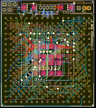
- Edited J1 silk label.

-To avoid risk of silk on pads I silked only the vias. prob woulda been fine but this wasn't hard and no doubts now.

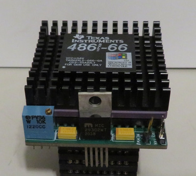
-Moved that resistor that was bugging me

-Rotated one of the edge caps.

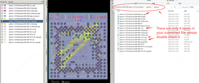
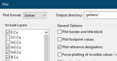
-Confirmed and fixed error in how the plotter was set up, those layers are checked now. for some reason it didn't check them automatically and I never noticed it.

-Added silk to vias of questionable proximity around the board as needed

-Unable to save as previous kicad file version as requested. sorry.

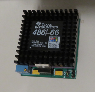
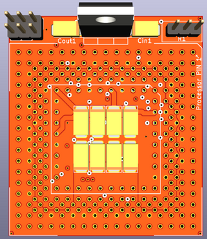
This pcb version is really nice, I'm liking where it is at. exciting!

-There are like 1,000 drc errors for silk screen now btw but it's fine. I knew that was gonna happen. shouldn't be an issue on physical object.

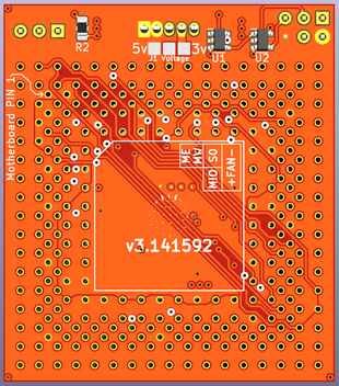
Feopia, are there any more concerns that I can address that you see on the physical part?

Attachments

  • Schematic.png
    Filename
    Schematic.png
    File size
    386.55 KiB
    Views
    642 views
    File license
    Public domain
  • front 3d.png
    Filename
    front 3d.png
    File size
    422.32 KiB
    Views
    642 views
    File license
    Public domain
  • back 3d.png
    Filename
    back 3d.png
    File size
    476.4 KiB
    Views
    642 views
    File license
    Public domain
Last edited by Sphere478 on 2022-11-02, 04:32. Edited 1 time in total.

Sphere's PCB projects.
-
Sphere’s socket 5/7 cpu collection.
-
SUCCESSFUL K6-2+ to K6-3+ Full Cache Enable Mod
-
Tyan S1564S to S1564D single to dual processor conversion (also s1563 and s1562)