VOGONS


Reply 20 of 94, by luckybob

User metadata
Rank l33t
Rank
l33t

Write back or write through? write back is usually faster on single cpu systems. Does that hold up on a dual cpu with a shared L2? Does it matter? Once I get my medication sorted out, ill be available to test. Until then I have to deal with these little pink Christina Aguilera monsters.

It is a mistake to think you can solve any major problems just with potatoes.

Reply 21 of 94, by Sphere478

User metadata
Rank l33t++
Rank
l33t++

I’ve concluded testing for a while I’ve taken apart the test bench that this was in and am now working on my p5a project.

As far as I can tell the board is not only stable, but working fine.

Catsay suggested checking the APIC this way

Both chips can't talk on the bus simultaneously anyways. If you want to check if your APIC is good, boot Linux and post the `dmesg` command output.

But I nuked the linux install and took apart the setup. i can check it later.

Catsay also said memtest detects shared bus bual processors as one processor so catsay thinks my observation is normal.

Anyway if your board is working in dual CPU mode without any IO related crashing and data corruption. Its pretty much confirmation that the APIC works

I only installed a sata card and radeon 7000 so this test will have to wait.

But it kinda seems like all is well. I do want to check linux though for that test eventually and learn what that row of SMDs do.

Catsay and shamano also hooked us up with this 430hx schematic which is pretty cool

Attachments

  • Filename
    430HX.pdf
    File size
    773.88 KiB
    Downloads
    98 downloads
    File license
    Public domain
Last edited by Sphere478 on 2021-12-24, 13:14. Edited 1 time in total.

Sphere's PCB projects.
-
Sphere’s socket 5/7 cpu collection.
-
SUCCESSFUL K6-2+ to K6-3+ Full Cache Enable Mod
-
Tyan S1564S to S1564D single to dual processor conversion (also s1563 and s1562)

Reply 22 of 94, by 0xCats

User metadata
Rank Newbie
Rank
Newbie

Catsay just jumping in here, to say this all looks pretty good.
Well done, great job on the dual socket conversion @Sphere478!

And about the 430HX/430NX boards, their design is maxed out at 512K of cache and 512MB of ram.
While the cache and memory controller could technically support enough address tags on it's external TAG address SRAM. the internal PCMC TAG status ram isn't large enough for storing all of the status bits.
The following emerges from the 430HX design notes:

430hx cache design notes.png
Filename
430hx cache design notes.png
File size
151.92 KiB
Views
2091 views
File license
Public domain

This effectively limits the board to 512K of Write-Back cache.
Also in general Intel advises that only Write-back cache be used on 430HX/NX platforms and in fact locks the chipset to a Write-Back policy. Write-through has horrible, and I mean catastrophic effects on a shared host bus architecture both for L2 and memory latency and bandwidth as well as crucially keeping track of cacheline state.
The reserved bits controlling the cacheline register when toggled only crash the system, and are simply undefined values in the register bit field.
They should also never be programmed directly, but are instead strapped and sampled at reset by the chipset on the Host Address Line 31.

In terms of DRAM the PCMCA has enough enough address bits to span up to 1GB of DRAM, however the external address lines as well as lack of necessary Row and Column strobe lines and other resource limits constrain the platform to 512MBytes.

There are two types of devices, those that know they've been hacked and those that don't yet know they're going to be hacked.

Reply 23 of 94, by 0xCats

User metadata
Rank Newbie
Rank
Newbie
Sphere478 wrote on 2021-12-23, 15:05:
Well, I got bored […]
Show full quote

Well, I got bored

Went ahead and just used the AMP socket.
8E86E56F-50E7-45FB-8153-38D347F48D54.jpeg6A2814C4-338B-4C1E-BF7F-6CFAA559CCA8.jpeg

I did notice this: but haven’t done anything about it yet67170689-57EE-4055-8E22-20B3BD17B66A.jpeg92BF016D-3AC8-4C16-91BF-D41CC4DA1D55.jpeg

It seems to post just fine but the RTC is being an issue.

I tried to start windows setup but it needs sata drivers, screw it. Gonna throw ubuntu on it and see what happensimage.jpg

This would most likely be one of the additional connections from the ISA or PCI interrupt lines being routed to the APIC chip.
You should be able to trace these out with a multimeter on your S1564D and check if they route to the same pad on your modified board.
Then replicate it to your modified board.

I put them side-by-side to more easily compare.

S1564D mode Sphere478.jpeg
Filename
S1564D mode Sphere478.jpeg
File size
86.57 KiB
Views
2086 views
File license
Public domain

But chances are you simply have to install the R276 0-ohm resistor or bridge it with a wire.

There are two types of devices, those that know they've been hacked and those that don't yet know they're going to be hacked.

Reply 24 of 94, by Sphere478

User metadata
Rank l33t++
Rank
l33t++
0xCats wrote on 2021-12-24, 12:29:
Catsay just jumping in here, to say this all looks pretty good. Well done, great job on the dual socket conversion @Sphere478! […]
Show full quote

Catsay just jumping in here, to say this all looks pretty good.
Well done, great job on the dual socket conversion @Sphere478!

And about the 430HX/430NX boards, their design is maxed out at 512K of cache and 512MB of ram.
While the cache and memory controller could technically support enough address tags on it's external TAG address SRAM. the internal PCMC TAG status ram isn't large enough for storing all of the status bits.
The following emerges from the 430HX design notes:
430hx cache design notes.png

This effectively limits the board to 512K of Write-Back cache.
Also in general Intel advises that only Write-back cache be used on 430HX/NX platforms and in fact locks the chipset to a Write-Back policy. Write-through has horrible, and I mean catastrophic effects on a shared host bus architecture both for L2 and memory latency and bandwidth as well as crucially keeping track of cacheline state.
The reserved bits controlling the cacheline register when toggled only crash the system, and are simply undefined values in the register bit field.
They should also never be programmed directly, but are instead strapped and sampled at reset by the chipset on the Host Address Line 31.

In terms of DRAM the PCMCA has enough enough address bits to span up to 1GB of DRAM, however the external address lines as well as lack of necessary Row and Column strobe lines and other resource limits constrain the platform to 512MBytes.

It’s interesting I can get the board to detect 768mb it counts all the way there. But it’s not usable and soon as you try to install a OS it crashes randomly. Like it’s reaching the end and overwriting the beginning or something idk. But I can confirm that 1gb and 768 definitely do not work. Despite the board having enough slots for it.

Someone suggested using 64mb sticks.

Do you think using all the banks would give any performance gain at all? Or same as 4x128?

0xCats wrote on 2021-12-24, 12:42:
This would most likely be one of the additional connections from the ISA or PCI interrupt lines being routed to the APIC chip. Y […]
Show full quote
Sphere478 wrote on 2021-12-23, 15:05:
Well, I got bored […]
Show full quote

Well, I got bored

Went ahead and just used the AMP socket.
8E86E56F-50E7-45FB-8153-38D347F48D54.jpeg6A2814C4-338B-4C1E-BF7F-6CFAA559CCA8.jpeg

I did notice this: but haven’t done anything about it yet67170689-57EE-4055-8E22-20B3BD17B66A.jpeg92BF016D-3AC8-4C16-91BF-D41CC4DA1D55.jpeg

It seems to post just fine but the RTC is being an issue.

I tried to start windows setup but it needs sata drivers, screw it. Gonna throw ubuntu on it and see what happensimage.jpg

This would most likely be one of the additional connections from the ISA or PCI interrupt lines being routed to the APIC chip.
You should be able to trace these out with a multimeter on your S1564D and check if they route to the same pad on your modified board.
Then replicate it to your modified board.

I put them side-by-side to more easily compare.
S1564D mode Sphere478.jpeg
But chances are you simply have to install the R276 0-ohm resistor or bridge it with a wire.

So you think that I’ll notice the problem there when I go to install a ISA card?

Thoughts on why we have discovered no less than three different configurations for those SMDs?

Do you think there is a danger in plugging in a isa card with it left as is?

How strongly do you recommend matching these to the D

Kinda hesitant to mess with it when it seems to be working, but if it’s a isa thing that makes sense why it would be fine since I’m not using isa

If you are sure that matching it is the right call I’ll do it. I have a scrap board I can rob SMDs from

Sphere's PCB projects.
-
Sphere’s socket 5/7 cpu collection.
-
SUCCESSFUL K6-2+ to K6-3+ Full Cache Enable Mod
-
Tyan S1564S to S1564D single to dual processor conversion (also s1563 and s1562)

Reply 25 of 94, by 0xCats

User metadata
Rank Newbie
Rank
Newbie
Sphere478 wrote on 2021-12-24, 12:45:

Someone suggested using 64mb sticks.

The boards are generally designed around a 64MB SIMM per slot maximum, as such half of the boards SIMM slots usually only have half the available RAS lines connected and/or are shared with primary slots.
This was a popular design decision back in the day when high density SIMM's were very rare and extremely costly
So the preference was to install a large number of 32/64MB modules.

In terms of performance there is not much difference to gain from having more selected rows, if anything on modern operating systems it actually becomes detrimental for this chipset to having lots of rows held open (asserted) by the memory controller. There should be a BIOS option to assert/deassert memory rows. This is what the memory controller does after accessing a memory row. If asserted is selected it will keep access memory rows held open for as long as possible to speed up subsequent access to that memory row. However in practice of testing on 430NX this has not borne out and only led me to very poor memory latency results. (I validated this with ChipsAndCheese and some image processing software under Alpine Linux)

If you would like, you can test the exact performance implications by using the ChipsAndCheese memory latency benchmark, which can be downloaded here:
https://github.com/ChipsandCheese/MemoryLaten … indows-i386.zip

https://github.com/ChipsandCheese/MemoryLatencyTest

Some results we have gathered can be found here, and as you can see for 430NX latency is pretty astronomical as is to be expected for such an old platform:

430NX latency.jpeg
Filename
430NX latency.jpeg
File size
81.04 KiB
Views
2075 views
File license
Public domain
actual time 430nx latency.png
Filename
actual time 430nx latency.png
File size
12.68 KiB
Views
2075 views
File license
Public domain

Though it is somewhat reasonable in terms of total cycles. Also the meaning of Asynchronous RAM becomes quite apparent when looking at the cycle count plot.
Memory latency doesn't scale with core frequency, because the ram runs asynchronously of the system clock at it's own speed, approx 25Mhz for FPM ram. This means at higher clock speeds, your CPU has a lot more idle cycles available where it can either do other things, or do nothing waiting for ram if it has nothing else to do.

cycles 430nx latency.png
Filename
cycles 430nx latency.png
File size
16.11 KiB
Views
2075 views
File license
Public domain
Last edited by 0xCats on 2021-12-24, 13:09. Edited 2 times in total.

There are two types of devices, those that know they've been hacked and those that don't yet know they're going to be hacked.

Reply 26 of 94, by 0xCats

User metadata
Rank Newbie
Rank
Newbie
Sphere478 wrote on 2021-12-24, 12:45:
So you think that I’ll notice the problem there when I go to install a ISA card? […]
Show full quote

So you think that I’ll notice the problem there when I go to install a ISA card?

Thoughts on why we have discovered no less than three different configurations for those SMDs?

Do you think there is a danger in plugging in a isa card with it left as is?

How strongly do you recommend matching these to the D

Kinda hesitant to mess with it when it seems to be working, but if it’s a isa thing that makes sense why it would be fine since I’m not using isa

If you are sure that matching it is the right call I’ll do it. I have a scrap board I can rob SMDs from

Ideally you would first just tone out with a multimeter where both sides of the connection of R276 come from.

The right side should run to a pin on the APIC.
The left side should run to one of the ISA bus pins.

Then you can lookup from the APIC datasheet and the ISA pinout what signal it deals with.

There are two types of devices, those that know they've been hacked and those that don't yet know they're going to be hacked.

Reply 27 of 94, by 0xCats

User metadata
Rank Newbie
Rank
Newbie

Just adding this while I'm at it.
Here is the 430HX PCISet design Guide document as well.
Have fun making your own 430HX board 😂

Merry Christmas everyone.

Attachments

  • Filename
    29746702.PDF
    File size
    823.07 KiB
    Downloads
    87 downloads
    File license
    Public domain

There are two types of devices, those that know they've been hacked and those that don't yet know they're going to be hacked.

Reply 28 of 94, by Sphere478

User metadata
Rank l33t++
Rank
l33t++
0xCats wrote on 2021-12-24, 19:42:
Just adding this while I'm at it. Here is the 430HX PCISet design Guide document as well. Have fun making your own 430HX board : […]
Show full quote

Just adding this while I'm at it.
Here is the 430HX PCISet design Guide document as well.
Have fun making your own 430HX board 😂

Merry Christmas everyone.

Lol when I posted it I forgot that it had already been posted, went back and added credit to OP

Sphere's PCB projects.
-
Sphere’s socket 5/7 cpu collection.
-
SUCCESSFUL K6-2+ to K6-3+ Full Cache Enable Mod
-
Tyan S1564S to S1564D single to dual processor conversion (also s1563 and s1562)

Reply 29 of 94, by Sphere478

User metadata
Rank l33t++
Rank
l33t++

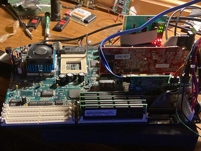
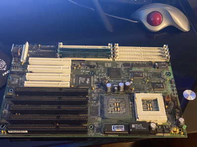
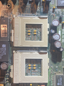
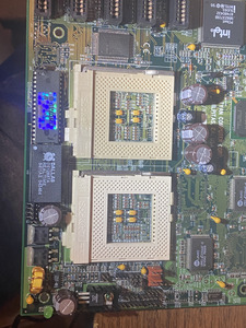
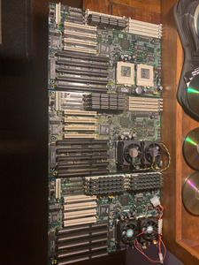
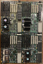
Got the k6-III+ running on the board. Unfortunately the k6-III+ In single is probably the fastest configuration that this motherboard supports. (Dual non intel doesn’t work, I’ve tried) Which is a shame to leave that socket open like that.

I’m thinking of making a 3d printed dummy cpu for the other socket 🤣 so I can install a heatsink and pretend that it’s there rofl.😂

I’ll probably put dual pentium back in it but for now, some k6 fun!

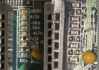
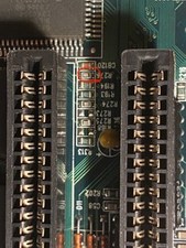
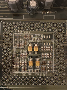
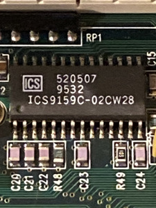
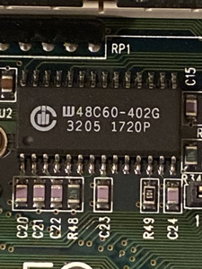
I still haven’t done anything with those resistors.

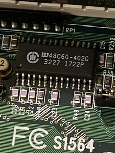
I have a third s1564 (a S) coming (I’m out of control)
I’m gonna compare it’s resistors and see if it matches the S, the D, or is yet a forth configuration.

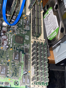
I’m about to install a few more cards to test it all out with as many cards as I can to make sure the irqs and whatnot are working. But I don’t have many ISA cards at my disposal so Idono how good of a test I can do.

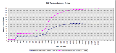
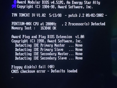
Interestingly I’m running it right now with the dual cpu jumper selected. I believe that means that it’s using the APIC I plan on doing some benchmarks external intel APIC vs internal cpu APIC later to see if there is a difference.

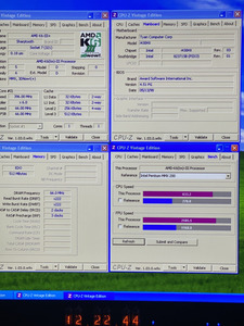
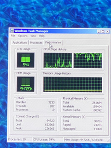
I tried to install this windows XP install using the mps multiprocessor kernel but it would hang at “setup is starting windows” whenever I tried it. If I just let setup select it’s own kernel it would work. So not sure which one it selected. Didn’t try others except the two mps uni/multiprocessor.

I wanted the mps kernel so that I could swap in two cpus without formatting. Oh well. If any of you have a suggestion on this I’m all ears.

Oh and btw, if you own this board and want to try the k6 2+/3+

These are the settings:
VD0 on, rest off
VIO on
j19 on, j20 off j21 off
J13 1-2 rest off

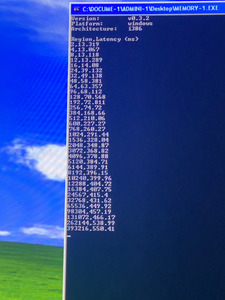
Bios sometimes detects as 366 or 400 depending on mood. Don’t worry it’s 396mhz or whatever. 😀 you’ll see in windows. You should use the latest Jan bios btw. Edit: I did notice it detecting 366 but actually being 396. And later I noticed 366 and it actually was 366. Not sure what’s up with this. Doesn’t make much sense. These all should be the correct jumper settings though. Why it’s flopping between 5.5x and 6x I haven’t a clue, perhaps a software glitch in the bios.

Which k6-2+/3+ you get doesn’t really matter as the fastest this board can run is 400mhz and all 2+/3+ models will work at that speed.

Attachments

Last edited by Sphere478 on 2022-01-04, 11:18. Edited 4 times in total.

Sphere's PCB projects.
-
Sphere’s socket 5/7 cpu collection.
-
SUCCESSFUL K6-2+ to K6-3+ Full Cache Enable Mod
-
Tyan S1564S to S1564D single to dual processor conversion (also s1563 and s1562)

Reply 30 of 94, by Sphere478

User metadata
Rank l33t++
Rank
l33t++

I got some time to look at these resistors a little closer

They are different colors yes, but this one (a 0 ohm link) seems to be the only actual difference between the D and The S

1A069A4D-D66D-4A39-A7AE-8A520EA30135.jpeg
Filename
1A069A4D-D66D-4A39-A7AE-8A520EA30135.jpeg
File size
16.85 KiB
Views
1954 views
File license
Public domain

I’m awaiting my 3rd board to compare it.

I did some testing with my k6 3+ and radeon 7000 and a bunch of cards

I had some stability issues which I think are probably more likely to do with drivers than anything else. It’s possible it may have been related to the k6 but I stopped testing that setup. Might come back around to it.

Sphere's PCB projects.
-
Sphere’s socket 5/7 cpu collection.
-
SUCCESSFUL K6-2+ to K6-3+ Full Cache Enable Mod
-
Tyan S1564S to S1564D single to dual processor conversion (also s1563 and s1562)

Reply 31 of 94, by Sphere478

User metadata
Rank l33t++
Rank
l33t++

I went back and removed that 0 ohm link from both the first one I converted and this one by the way. As this one also had that difference it seemed logical that it should be removed if both S models had it and the D did not.

Here are the pics from the conversion of the second s1564s (my third s1564) board:

DE4788A7-518F-4C17-93A0-9EAF0F1F7B29.jpeg
Filename
DE4788A7-518F-4C17-93A0-9EAF0F1F7B29.jpeg
File size
1.52 MiB
Views
1934 views
File license
Public domain

As it arrived^

AF9BB796-6124-47E0-9B94-7144100DB6BA.jpeg
Filename
AF9BB796-6124-47E0-9B94-7144100DB6BA.jpeg
File size
1.61 MiB
Views
1934 views
File license
Public domain

Holes cleaned out with hot air and vacuum cleaner^

21313B2B-3906-49A8-8CB1-7E6A8B0CAE36.jpeg
Filename
21313B2B-3906-49A8-8CB1-7E6A8B0CAE36.jpeg
File size
1.84 MiB
Views
1934 views
File license
Public domain

the mess that the vacuum cleaner left and work begun^ not to worry about the mess. Not much point in cleaning up i can re use that while I work!^

F2C6ED44-6DF2-4937-AC7B-FD0155485D7D.jpeg
Filename
F2C6ED44-6DF2-4937-AC7B-FD0155485D7D.jpeg
File size
1.9 MiB
Views
1934 views
File license
Public domain

Looking good, more cleanup to do though!^

D2B91E12-B97F-4CA1-8B79-33B2B91D4845.jpeg
Filename
D2B91E12-B97F-4CA1-8B79-33B2B91D4845.jpeg
File size
1.76 MiB
Views
1934 views
File license
Public domain

It’s in!

Last edited by Sphere478 on 2022-01-05, 09:40. Edited 2 times in total.

Sphere's PCB projects.
-
Sphere’s socket 5/7 cpu collection.
-
SUCCESSFUL K6-2+ to K6-3+ Full Cache Enable Mod
-
Tyan S1564S to S1564D single to dual processor conversion (also s1563 and s1562)

Reply 32 of 94, by Sphere478

User metadata
Rank l33t++
Rank
l33t++
3DE5AF49-1264-4550-B02E-D6362BD91712.jpeg
Filename
3DE5AF49-1264-4550-B02E-D6362BD91712.jpeg
File size
1.68 MiB
Views
1926 views
File license
Public domain

Preparing pad, I also fluxed up the chip pins and added small bit of solder to them^

4D63C7B9-F760-4F17-8CC4-AAEDA5C4AA23.jpeg
Filename
4D63C7B9-F760-4F17-8CC4-AAEDA5C4AA23.jpeg
File size
1.82 MiB
Views
1926 views
File license
Public domain

APIC installed!^ last time I used hot air, this time a iron, both times it affected the plastic of the isa slot, perhaps hot air on the non isa side and iron on the isa side may be best way (some aluminum tape as a heat shield may have been a good idea also). Be sure to push down on chip while soldering, now to check that all the pins were soldered well and clean it up!^

Next (off camera) I used a magnifying glass, tweasers, brass wire brush, and a pressure washer to scrape, blow, brush away all remaining chunks of flux

Then a air gun to blow the water out from under all the chips and sockets on the board, followed by a hair dryer to bake it dry

67453B9D-6278-4BE0-BF27-F74D4B2576E2.jpeg
Filename
67453B9D-6278-4BE0-BF27-F74D4B2576E2.jpeg
File size
1.83 MiB
Views
1926 views
File license
Public domain
7BD99ECA-ACC1-43EB-B073-1D97F5967CFB.jpeg
Filename
7BD99ECA-ACC1-43EB-B073-1D97F5967CFB.jpeg
File size
1.83 MiB
Views
1926 views
File license
Public domain

Some pics of the final product.^

Last edited by Sphere478 on 2022-01-06, 09:50. Edited 3 times in total.

Sphere's PCB projects.
-
Sphere’s socket 5/7 cpu collection.
-
SUCCESSFUL K6-2+ to K6-3+ Full Cache Enable Mod
-
Tyan S1564S to S1564D single to dual processor conversion (also s1563 and s1562)

Reply 33 of 94, by Sphere478

User metadata
Rank l33t++
Rank
l33t++

One final order of business, update to latest Jan bios!

93BA3F0F-7990-4970-874F-9740AD37B656.jpeg
Filename
93BA3F0F-7990-4970-874F-9740AD37B656.jpeg
File size
1022.86 KiB
Views
1916 views
File license
Public domain

Three of these boards now and I swear three different mfgs, 🤣 I think the pn is the same though. So may be able to try this before peeling your sticker. I like to keep my stickers on.

ITZ ALIVE!!!

1594EF97-7DC1-4414-820C-BF0D2D6A08BC.jpeg
Filename
1594EF97-7DC1-4414-820C-BF0D2D6A08BC.jpeg
File size
1.3 MiB
Views
1916 views
File license
Public domain

Sphere's PCB projects.
-
Sphere’s socket 5/7 cpu collection.
-
SUCCESSFUL K6-2+ to K6-3+ Full Cache Enable Mod
-
Tyan S1564S to S1564D single to dual processor conversion (also s1563 and s1562)

Reply 34 of 94, by Sphere478

User metadata
Rank l33t++
Rank
l33t++

Took me a few days, but we have proof of life!

image.jpg
Filename
image.jpg
File size
1.25 MiB
Views
1880 views
File license
Public domain

Just to be sure I like to run super pi while stressing the other cpu with cpuz and play around with realtime priority and affinity. We all know how unresponsive a single cpu system will become if you set something like super pi to realtime priority, pretty good proof that your dual cpu system is working if you can still move windows around after doing that.

I still remain confused as to how the ram on this board is supposed to be installed because 512 total in slots 1-4 works but this is how 384 works with 2x128 and 4x32 (perplexing)

581A43AE-2436-44D1-930F-598AEE5F0EF3.jpeg
Filename
581A43AE-2436-44D1-930F-598AEE5F0EF3.jpeg
File size
1.86 MiB
Views
1861 views
File license
Public domain

I’ve noted on this board that when checking memory stick configuration you must use unique data, not just memtest programs. Sometimes memtest won’t detect stick installation anomalies, it’s more of a “is the stick stable?” Rather than a “are all the data lines and sticks in the right place to make a full and functional bank of memory?” Kinda program.

I opened up the driver .cab file on the xpsp3 disk and coppied it’s contents to a new folder on the desktop to test this configuration it fully filled the ram and even spilled over onto page without error. So looks like it’s configured properly. Now I can move on to memory timing tweaks. For that I’ll use memtest.

edit:
I swapped with the other converted board and it wasn't being as picky with memory. I think it may have been a bios setting or maybe a solder blob somewhere because while swapped out I blew it out again really good with the air gun after confirming the other board was much more friendly to memory configurations. anyway I put he board back in ( the one with the memory issues) and changed some bios settings which were set to the most lax and now it works fine which is how the other one was set (more agressive) anyway I think it was probably a bios setting maybe cachable area? not sure. all boards are fully working though!

Sphere's PCB projects.
-
Sphere’s socket 5/7 cpu collection.
-
SUCCESSFUL K6-2+ to K6-3+ Full Cache Enable Mod
-
Tyan S1564S to S1564D single to dual processor conversion (also s1563 and s1562)

Reply 35 of 94, by Sphere478

User metadata
Rank l33t++
Rank
l33t++

I’ve now converted three boards. (Pictured) plus one true Dual board that is in a computer still. So basically I have 4 now 🤣.

It’s pretty routine now, socket, apic, resistor, jumper, bios, clean, test.

I’ve settled on the 375f setting on the hot air it seems to be a good setting that is hot but not too hot that it burns the board but I am only using it for desoldering the socket, I am now doing everything else by iron and flux.

Oh, aluminum tape on the isa slot is a good idea, to keep the iron from melting it.

I’m liking the celeron heatsinks. But the clips suck. Be careful they don’t hurt the resistors between primary socket and cache. If installed without care for that, they are leveraged to cause damage there.

I think my previous memory issues may have been due to mismatched groups of sticks. They were matched pairs but the pairs didn’t match the other pairs.

The board is picky about the ram. Unpacking driver.cab seems to be a very good test for checking the ram configuration on this board, followed by memtest of course.

I also harvested my first socket.

I used a torch on the back of a parts board.
I put a heatsink on the socket with a processor in it and closed it. Then basically burnt the back of the board to a crisp in about 10 seconds.before the socket fell off. Socket was in perfect shape! Board, not so much 🤣. I suspected being quick was more important than saving the parts board. Results were favorable.🤷‍♂️

Attachments

Last edited by Sphere478 on 2022-02-08, 04:15. Edited 1 time in total.

Sphere's PCB projects.
-
Sphere’s socket 5/7 cpu collection.
-
SUCCESSFUL K6-2+ to K6-3+ Full Cache Enable Mod
-
Tyan S1564S to S1564D single to dual processor conversion (also s1563 and s1562)

Reply 36 of 94, by Sphere478

User metadata
Rank l33t++
Rank
l33t++

Had the oem dual board out today and decided to take a family photo 🤣

BF6E0153-445F-4C06-80EF-77D2324DB52A.jpeg
Filename
BF6E0153-445F-4C06-80EF-77D2324DB52A.jpeg
File size
1.45 MiB
Views
1813 views
File license
Public domain

Also noticed this,

C834B069-A182-48BD-9383-D4EE748193B0.jpeg
Filename
C834B069-A182-48BD-9383-D4EE748193B0.jpeg
File size
973.76 KiB
Views
1810 views
File license
Public domain
F8BA4180-80CD-4E15-BC7D-F2F917716DB8.jpeg
Filename
F8BA4180-80CD-4E15-BC7D-F2F917716DB8.jpeg
File size
1.09 MiB
Views
1810 views
File license
Public domain
61BA6CEF-F8DA-4021-BCAB-EFC8FEEC2313.jpeg
Filename
61BA6CEF-F8DA-4021-BCAB-EFC8FEEC2313.jpeg
File size
878.82 KiB
Views
1810 views
File license
Public domain
1A93BE17-16AB-4989-B4BF-8BDC331AD4CD.jpeg
Filename
1A93BE17-16AB-4989-B4BF-8BDC331AD4CD.jpeg
File size
998.85 KiB
Views
1810 views
File license
Public domain

Sphere's PCB projects.
-
Sphere’s socket 5/7 cpu collection.
-
SUCCESSFUL K6-2+ to K6-3+ Full Cache Enable Mod
-
Tyan S1564S to S1564D single to dual processor conversion (also s1563 and s1562)

Reply 37 of 94, by snufkin

User metadata
Rank Oldbie
Rank
Oldbie

Just been exchanging a few message with Sphere about that R276 0-ohm link that's fitted on boards without the APIC, and what it might be doing, and it was suggested it'd be useful to post this here. I should say that I don't know anything about dual processors or SMI.

Why mention SMI? Downloading the partial APIC datasheet from here: http://www.datasheetcatalog.com/datasheets_pd … 9/82093AA.shtml then it looks like R276 goes between pins 6 (SMIOUT) and 44 (SMI# interrupt input).

So, with no APIC fitted and R276 fitted then a signal can come in from the right in the picture (from the chipset?), through R276, where it then splits and heads up in the direction of the KBC and down toward the CPUs. Don't know where it actually goes, but I'm assuming it connects to their SMI# pins (AB34?). With an APIC fitted and R276 removed, then the signal comes in and goes to the APICs SMI input. It's then up the APIC to trigger the SMIOUT and pass the signal on. Maybe there's some way to trigger just one CPU?

Wikipedia entry on SMI stuff, which taught me everything I know about it: https://en.wikipedia.org/wiki/System_Management_Mode

Attachments

  • Tyan_s1564_SMI.jpg
    Filename
    Tyan_s1564_SMI.jpg
    File size
    125.49 KiB
    Views
    1797 views
    File license
    Fair use/fair dealing exception

Reply 38 of 94, by Sphere478

User metadata
Rank l33t++
Rank
l33t++
snufkin wrote on 2022-02-07, 21:12:
Just been exchanging a few message with Sphere about that R276 0-ohm link that's fitted on boards without the APIC, and what it […]
Show full quote

Just been exchanging a few message with Sphere about that R276 0-ohm link that's fitted on boards without the APIC, and what it might be doing, and it was suggested it'd be useful to post this here. I should say that I don't know anything about dual processors or SMI.

Why mention SMI? Downloading the partial APIC datasheet from here: http://www.datasheetcatalog.com/datasheets_pd … 9/82093AA.shtml then it looks like R276 goes between pins 6 (SMIOUT) and 44 (SMI# interrupt input).

So, with no APIC fitted and R276 fitted then a signal can come in from the right in the picture (from the chipset?), through R276, where it then splits and heads up in the direction of the KBC and down toward the CPUs. Don't know where it actually goes, but I'm assuming it connects to their SMI# pins (AB34?). With an APIC fitted and R276 removed, then the signal comes in and goes to the APICs SMI input. It's then up the APIC to trigger the SMIOUT and pass the signal on. Maybe there's some way to trigger just one CPU?

Wikipedia entry on SMI stuff, which taught me everything I know about it: https://en.wikipedia.org/wiki/System_Management_Mode

Thanks so much!, this was bugging me, glad we have a answer. It feels like that was the final mystery left for this conversion. Even with several successes, it still bugged me not understanding that resistor and it’s function.

Sphere's PCB projects.
-
Sphere’s socket 5/7 cpu collection.
-
SUCCESSFUL K6-2+ to K6-3+ Full Cache Enable Mod
-
Tyan S1564S to S1564D single to dual processor conversion (also s1563 and s1562)

Reply 39 of 94, by Sphere478

User metadata
Rank l33t++
Rank
l33t++
0xCats wrote on 2021-12-24, 12:59:
The boards are generally designed around a 64MB SIMM per slot maximum, as such half of the boards SIMM slots usually only have h […]
Show full quote
Sphere478 wrote on 2021-12-24, 12:45:

Someone suggested using 64mb sticks.

The boards are generally designed around a 64MB SIMM per slot maximum, as such half of the boards SIMM slots usually only have half the available RAS lines connected and/or are shared with primary slots.
This was a popular design decision back in the day when high density SIMM's were very rare and extremely costly
So the preference was to install a large number of 32/64MB modules.

In terms of performance there is not much difference to gain from having more selected rows, if anything on modern operating systems it actually becomes detrimental for this chipset to having lots of rows held open (asserted) by the memory controller. There should be a BIOS option to assert/deassert memory rows. This is what the memory controller does after accessing a memory row. If asserted is selected it will keep access memory rows held open for as long as possible to speed up subsequent access to that memory row. However in practice of testing on 430NX this has not borne out and only led me to very poor memory latency results. (I validated this with ChipsAndCheese and some image processing software under Alpine Linux)

If you would like, you can test the exact performance implications by using the ChipsAndCheese memory latency benchmark, which can be downloaded here:
https://github.com/ChipsandCheese/MemoryLaten … indows-i386.zip

https://github.com/ChipsandCheese/MemoryLatencyTest

Some results we have gathered can be found here, and as you can see for 430NX latency is pretty astronomical as is to be expected for such an old platform:
430NX latency.jpeg

actual time 430nx latency.png

Though it is somewhat reasonable in terms of total cycles. Also the meaning of Asynchronous RAM becomes quite apparent when looking at the cycle count plot.
Memory latency doesn't scale with core frequency, because the ram runs asynchronously of the system clock at it's own speed, approx 25Mhz for FPM ram. This means at higher clock speeds, your CPU has a lot more idle cycles available where it can either do other things, or do nothing waiting for ram if it has nothing else to do.

cycles 430nx latency.png

I finally got around to doing this test on a dual 233 (this is the oem dual not that I think there is any difference) with 4x128mb in 1,2,3,4.

Does this tell anything useful?

Attachments

Sphere's PCB projects.
-
Sphere’s socket 5/7 cpu collection.
-
SUCCESSFUL K6-2+ to K6-3+ Full Cache Enable Mod
-
Tyan S1564S to S1564D single to dual processor conversion (also s1563 and s1562)