VOGONS


First post, by crazytiti

User metadata
Rank Newbie
Rank
Newbie

Hello,
At first i want to show my respect for the highly technical stuff that i already read on this forum, you guys seems to know what you're doing !
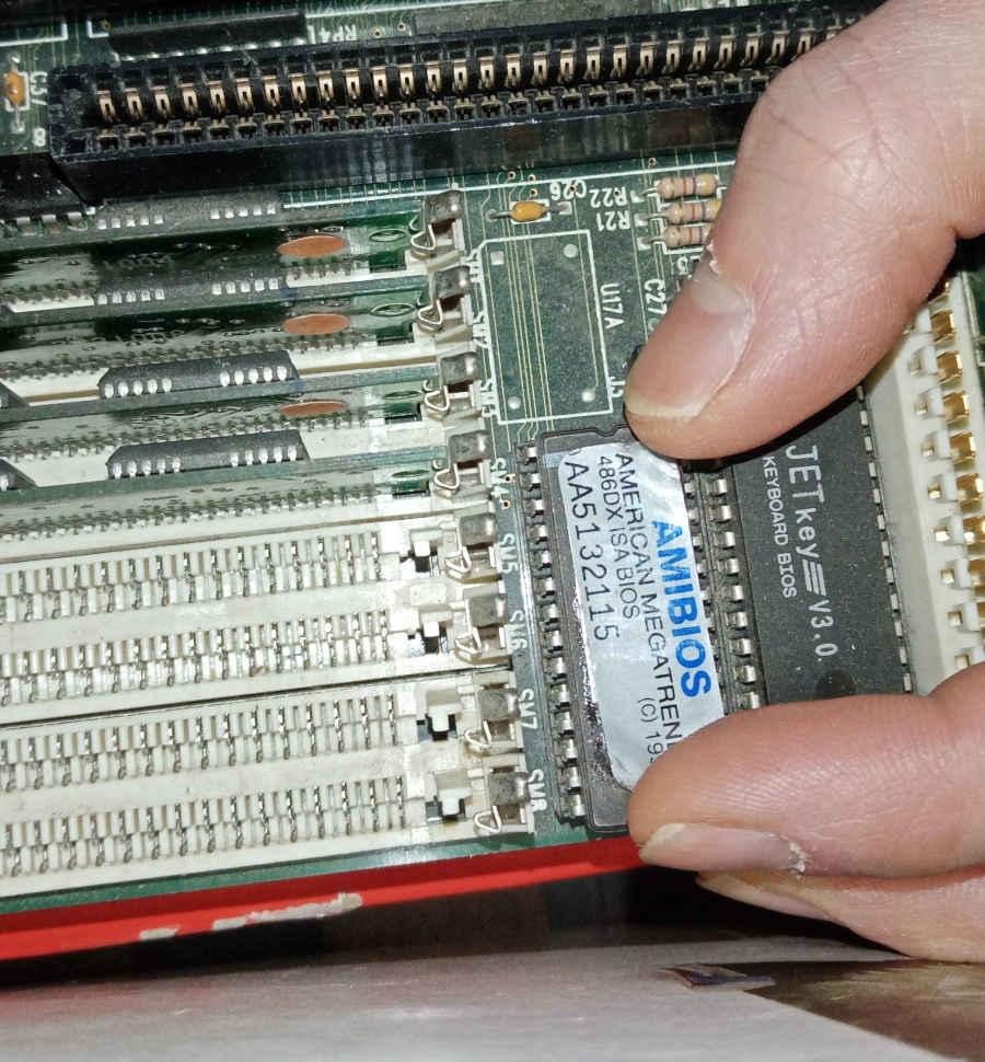
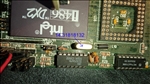
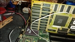
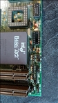
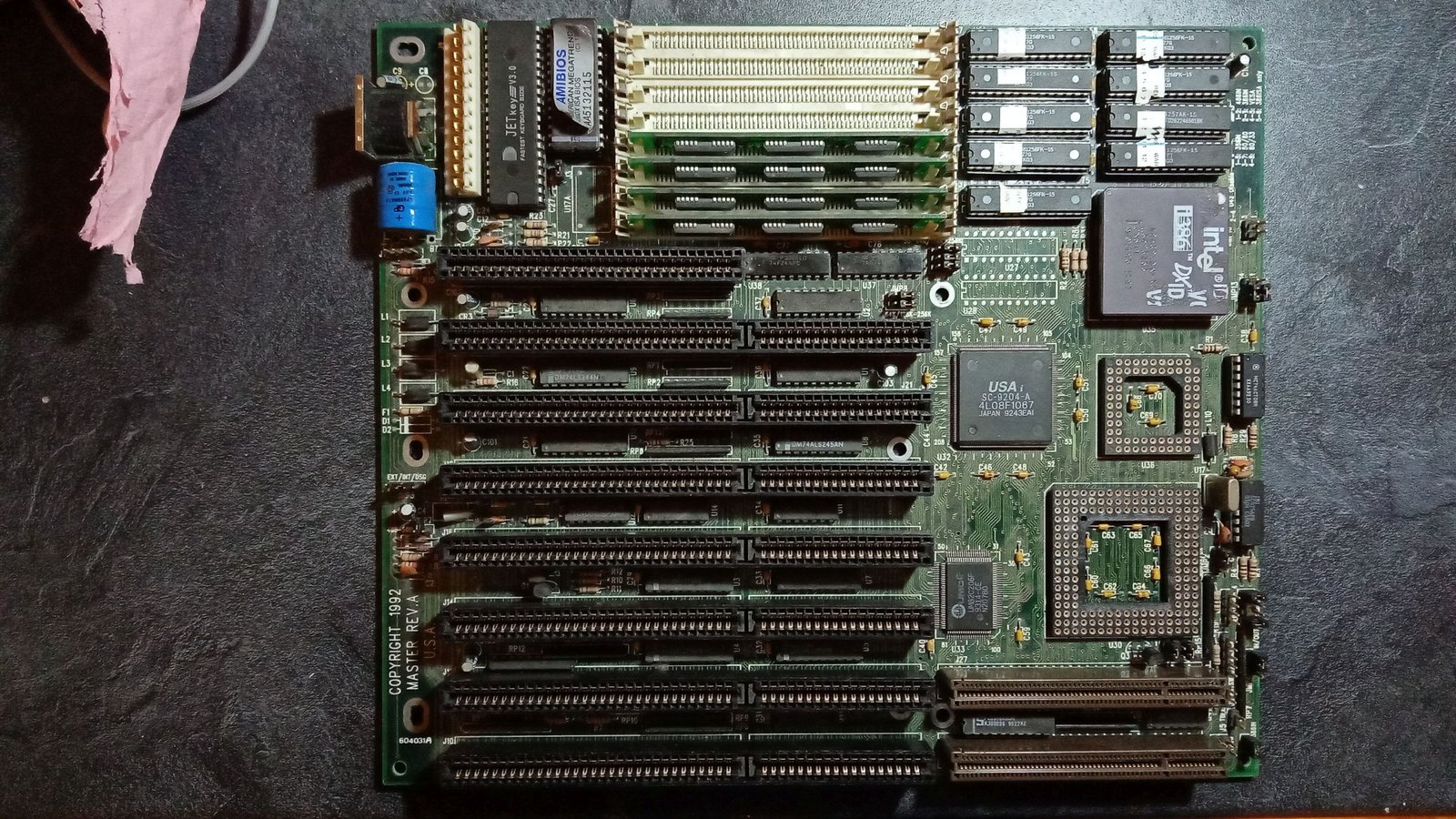
I try to revive an old 386/486 motherboard that some friends on forum.hardware.fr help me to identify as a 786 VESA motherboard :
https://stason.org/TULARC/pc/motherboards/U/U … VESA-VER-2.html
I have multiple cpu to put on it : 386 dx, 486 dx33, 486dx-2-66 and 486 dx4 120 (amd) but i think the last one cannot be put because of the 3.3V it need.
Now the problem : the card does not boot, not beep, nothing.
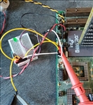
I try to put an ISA/PCI debug card on it but it show nothing (not light at all)
I suspect the bios to have lost its content.
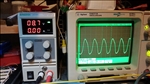
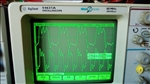
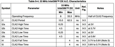
I have some electronics and computer skills nontheless, i can make electronics measurement, i could find a way to flash uvprom, i can solder things on motherboard, i even have 200mhs dual scope if needed.
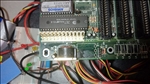
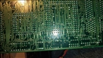
The motherboard.
210421123509346720.jpg
210529033054536861.jpg
Ps : all my apologies if i'm in the wrong topic.

Reply 1 of 46, by snufkin

User metadata
Rank Oldbie
Rank
Oldbie

No lights on the POST card suggests there's no power getting to the slot, and that doesn't depend on the BIOS. Can you measure the all the voltages on the main AT connector relative to the black Ground wires?

Also, remove the barrel battery and make sure it hasn't leaked and taken out any PCB traces. Then fit an external CMOS battery.

Reply 2 of 46, by Eep386

User metadata
Rank Member
Rank
Member

Also make sure you didn't put the POST probe card into a slot that has corroded pins. Varta bombs (and GP leakers) love to demolish nearby ISA slots.

I suspect that 'USA' chipset is an OPTi of some kind. It's got a very similar look to it, right down to the Toshiba-style fab markings. (Toshiba fabbed a lot of chips for other makers too, so Toshiba is far from exclusive to OPTi. However, many of OPTi's 82C495 series were fabbed by Toshiba, so I felt I should mention that.)

Life isn't long enough to re-enable every hidden option in every BIOS on every board... 🙁

Reply 3 of 46, by crazytiti

User metadata
Rank Newbie
Rank
Newbie

Oh i forgot to mention that when testing the cpu ran a little warm, so it's powered.
I just had the occasion to test the POST card on a known working H-P vectra P133, and it's not working in the ISA slot, even preventing the system to boot ! Working fine in the PCI slot.
So this A311L5G1112 is out of the way for debugging (i also found this Troubles between a PCI/ISA POST card and my Asus P55T2P4-C motherboard post and i can assure i put it in the right direction)
I also manage to test the wd89c00 video card, working at boot and in 16 color 640*480 in windows98 (i didn't try to put correct driver on it)
So far i know :
PSU is OK
VGA card OK
CPU ?? (i have several but all are ??)
motherboard ?? (but i greatly think the uvprom is erased since the sticker was unglued)
The slots seems to be ok with no visible corrosion.
The jumper are setting for 386 which is on it at that time (i've already test with the dx2-66 too)

Edit : here is the bios sticker
58977

Reply 4 of 46, by crazytiti

User metadata
Rank Newbie
Rank
Newbie

I check the bios, i think it's me some time ago that unglue the sticker because under their is an aluminum tape to protect the eeprom !
I have read the bios and it's seems OK, i've uploaded it, if someone with AMI bios knowledge could check it :
http://crazytiti.free.fr/divers/AMIBIOS%20486 … 115%20c1992.rom

I even find the AMI bios ID in the bios :
40-1200-001805-00101111-060692-USA-9204

59113

Reply 5 of 46, by snufkin

User metadata
Rank Oldbie
Rank
Oldbie

Huh, based on that BIOS string it turns out the board's very similar to https://www.ultimateretro.net/en/motherboards/6714#downloads but it has a different manufacturer code.

[edit: that page says it has a relabeled Toshiba chipset]
[also this: https://www.ultimateretro.net/en/motherboards/9801 , but this has different jumpers, closer to https://www.ultimateretro.net/en/motherboards/5462 ]
[and of course this: https://www.ultimateretro.net/en/motherboards/5461 ]

Not sure where best to start looking. Check voltages on the BIOS chip and use scope to look for activity on the address lines? Check for a clock signal on the 386 socket?

Reply 6 of 46, by crazytiti

User metadata
Rank Newbie
Rank
Newbie

I ran some tests tonight :
Put an 486 dx33
- Bios voltage OK, but address and data lines are stuck
- Battery voltage was originally ~2V, 4V when powered, 3.8 at rest.
- i measure "clock" pin on 386 socket (the one next to the "key pin) and got continuous 0V or 5V or 1.9V randomly each time i powered on the system.
- the Power Led and Turbo Led are OFF
- Cpu is a little warm, as the GPU (can i call it like that ?) so power is going somewhere at least !
- i try without any ram and without any cache : nothing change
- try with a 486 dx2-66 : nothing new
- i un-soldered the battery : trace are OK (see pictures), but nothing better
So i think clock management isn't working, any idea ? there's a little 2 pin ~14.xxxMhz quartz next to the speed jumpers and another small cylindrical one between two isa slots.
59229
59230

Reply 7 of 46, by snufkin

User metadata
Rank Oldbie
Rank
Oldbie

The one near the CPU sockets will be the main clock, the small cylinder will be a 32.768kHz for the RTC. Have you got a photo showing near the 14.318 crystal? That is probably buffered through a clock buffer nearby, so would be a good place to look for an active clock.

Looks like the battery has leaked, there's some gunky looking stuff around the keyboard connector. Probably a good idea to give the board a wash in that area. You might also want to remove the keyboard, power and J7 connectors to clean underneath them.

Reply 8 of 46, by crazytiti

User metadata
Rank Newbie
Rank
Newbie

Ok i already do a little wash with 90°alcohol and a toothbrush, but you're right it need more.
Although i thought the battery to be relatively clean.
Here are two picture (front and back) of the surrounding of the quartz, is the SC425APB relevant ?
I didn't find the correct datasheet 😒
Edit : https://datasheet.datasheetarchive.com/origin … AIH00054001.pdf
59249 59250
59247 59248

Reply 9 of 46, by snufkin

User metadata
Rank Oldbie
Rank
Oldbie

[edit: ah, I missed that you found the actual data sheet, nice. So check pins 8,11 & 13 for clock signals]

Found an overview of the SC4xx family of clock gen chips: https://www.datasheetarchive.com/pdf/download … pe=O&term=SC425

That has lots of useful information for the SC425, but no actual pinout. But from that we know there are 3 clock outputs: Reference (@14.318MHz), MCLK1 (half MCLK2) and MCLK2 (selected by S0-3, with S3 looking like the turbo input).

Wild stab, but looking at this: https://www.ultimateretro.net/motherboard/manual/31843.pdf my guess is that JMP9 1-5 connects the clock to the 386 socket. 2-6, 3-7 and 4-8 somehow control S0 and S1, but I can't see how. JMP14 might have something to do with wait states on the VLB slots when running at 50MHz.

So, if you set the board for a 386/25MHz (JMP9 1&5,2&6) then you should find 3 pins on the SC425 with clocks, one at 14.318MHz, one at 24MHz (they cheat you out of 1MHz) and one at 12MHz, and you should find a clock on the 386 socket. Remove 1&5 and the clock to the 386 socket might disappear. Move the jumper to 4&8 (as I think it is now) and you should find the 24 and 12 clocks change to 32 and 16.

[Oh, and the white crystalline stuff on the battery is a sign that it's leaked, along with the green corrosion. And that stuff will sit on the board slowly eating at anything metal. Vinegar is apparently a good way to shift it (acid against the alkali battery fluid), then water to wash the vinegar away, then IPA to flush out the water and dry the board off.]

Reply 10 of 46, by crazytiti

User metadata
Rank Newbie
Rank
Newbie

Ok so i have tested a few thing and i'm afraid that this motherboard is deadly dead 😒
After some cleaning i can tell that the trace under the keyboard connector and J7 are ok
So i have run a few test :
The SC425APB does not generate a valid clock : on the Ref pin signal is OK but MCLK1 and 2 are garbage.
Then this garbage goes to an AND gate (74ACT08) and the output of the and go to the two socket.
I then proceed to do Frankenstein stuff : i unplug the faulty? SC425 and run a wire from a 28MHZ clock of my video card.
But the system still does not beep, boot, show something on screen, nor does it turn the power led on.
I'm a little desperate and afraid of multiple issues on this board.
It's sad because it's OK looking, nothing broke, burn or scratch...

Note : i did not have the ability to generate the second MCLK together maybe it's needed ?

Clock Ref
59306
MCLK1
59308
Frankenstein mod
59307
Frankenstein Clock on socket
59309

Reply 11 of 46, by snufkin

User metadata
Rank Oldbie
Rank
Oldbie

Well, that looks like a possible cause of the board not working. Very likely the board will need the reference clock, and probably both MCLK1&2 (chipset may need a half clock, maybe?). You can see traces and a via going from pins 11 (MCLK1) and 13 (REF), so very likely they are used somewhere.

[edit: oh, and I think MCLK2, pin 8) is the main CPU clock. MCLK1, pin 11, is MCLK2/2]

Check the voltage on the inputs to the clock chip, particularly the S0-3 pins, and the TS pin. Also, maybe there's something up with what should be a 0.1uF capacitor between pins 6&7, apparently part of the PLL feedback. Maybe the chip can't get a lock on the reference.

If the chip is at fault then a direct replacement will be tricky to find, but you might be able to cobble something together using another clock gen chip, although the range of frequencies might be limited. I know there are a few chips that have reference, 24 and 12MHz fixed outputs, plus a bunch of outputs you don't need (CGS605, ICS9159-02, W48C60-402, CY2254). If you can find one of those you can at least see if there's any sign of life from the board.

When you say power LED, do you mean on a header? I would have thought the header would just be two pins, one with a resistor connected to +5 and the other the Ground. So if that's not on then either the resistor's gone, or the +5 isn't present, or the connector's back to front, or the LED is dead.

Reply 12 of 46, by crazytiti

User metadata
Rank Newbie
Rank
Newbie

Yes it's MCLK2 that is going to the AND gate.
I've checked all the voltage on the SC425 inputs and they're OK.
But the PD ouput is a continuous 0.5V so the phase detection does not work/lock.
I've also un-solder the 0.1µF and measure it (0.077) replace it with a brand new 0.1 and ... nothing change, so i resolder the old one (better size than my replacement)
Thank you for the reference of clock chips.
I will try to generate clock and clock/2 with an arduino, i should be able to get something between 4-12mhz which should be sufficient to see if it works.
By power Led i mean on J2 "power led and key lock", i try both direction but the first two pin always read 0 even with the voltmeter.
Same for the turbo led.
I find this very odd as the 5V goes throught CPU and, at least, the SC425 and 74ACT08.
Maybe they're driven by cpu or bios ?
By the way was is the role of the "JETKEY bios keyboard" chip next to the UVPROM ?
Are the bios settings saved inside this chips ?

Reply 13 of 46, by snufkin

User metadata
Rank Oldbie
Rank
Oldbie

Ok, so more evidence of likely at least a bust clock gen.

crazytiti wrote on 2022-01-16, 09:22:

Yes it's MCLK2 that is going to the AND gate.

So it looks like all three clocks are needed.

I've checked all the voltage on the SC425 inputs and they're OK. But the PD ouput is a continuous 0.5V so the phase detection do […]
Show full quote

I've checked all the voltage on the SC425 inputs and they're OK.
But the PD ouput is a continuous 0.5V so the phase detection does not work/lock.
I've also un-solder the 0.1µF and measure it (0.077) replace it with a brand new 0.1 and ... nothing change, so i resolder the old one (better size than my replacement)
Thank you for the reference of clock chips.
I will try to generate clock and clock/2 with an arduino, i should be able to get something between 4-12mhz which should be sufficient to see if it works.

That should work. There'll be some lower limit on the clock speed, but I'd expect a 12 & 6 to work. I haven't done arduino programming, but try to make sure you keep them as close to in phase as you can. Probably not a problem since I guess you can write to a GPIO register to change two outputs at the same time.

By power Led i mean on J2 "power led and key lock", i try both direction but the first two pin always read 0 even with the voltm […]
Show full quote

By power Led i mean on J2 "power led and key lock", i try both direction but the first two pin always read 0 even with the voltmeter.
Same for the turbo led.
I find this very odd as the 5V goes throught CPU and, at least, the SC425 and 74ACT08.
Maybe they're driven by cpu or bios ?

Since there's the header on the motherboard then I'd expect the turbo LED to be controlled by the chipset. Probably means there's some key combination to switch turbo off and on, which the board can then give a signal to the user about the current state. Slightly surprised the power LED might also be controlled by the chipset. Have you got a photo of the jumper area?

By the way was is the role of the "JETKEY bios keyboard" chip next to the UVPROM ?
Are the bios settings saved inside this chips ?

Keyboard controller. For reasons (I don't know) the original AT had a separate processor (Intel 8042) for the keyboard, and that's stayed. Probably helps to have something that's pretty much guaranteed to be still be working and able to reset the CPU if a program has crashed, plus there was something about switching modes on the 286.

I don't know where this board will store the CMOS settings. Sometimes it's in the chipset, sometimes there'll be a small SRAM chip somewhere, sometimes a Dallas RTC/CMOS chip. It has to get some power from the battery, so look for anything with connections to the +ve battery terminal. Since there's no obvious RTC chip then I guess it's stored in the chipset.

Ah, looking at the UMC 82C205 datasheet, then that has the RTC and CMOS SRAM inside. Pin 75 should have a 32.768kHz clock going in to it, pin 78 (one of several Vcc pins) should have some voltage from either board or battery when the board is off.

Reply 14 of 46, by crazytiti

User metadata
Rank Newbie
Rank
Newbie

Thanks for the explanations 😀
So i get an ATtiny85 which has ability to toggle pin in one cycle, i make two signals 8 and 4Mhz in phase
59345
i plug it in MCLK2, 1 and REF (i use the 8mhz to put in REF)
59347
The signals have "good" waveform when plugged, so impedance and current capability of ATtiny where good enough.
59348
But, nothing change, no beep, no power led and nothing at screen
I found a ~230 ohms resistor (R20) from one pin of Power led to ground. At least now i know in which way i have to plugged it...
59349

Reply 15 of 46, by snufkin

User metadata
Rank Oldbie
Rank
Oldbie
crazytiti wrote on 2022-01-16, 14:39:

I found a ~230 ohms resistor (R20) from one pin of Power led to ground. At least now i know in which way i have to plugged it...

Hmm, having a quick look around I'd expect that the pinout of the header would be: 1) LED +5V, 2) N/C, 3) LED GND, 4)Keyboard lock, 5)Klock GND

Colour bands on R20 look like 150 ohm (brown-green-brown?) so there some extra resistance somewhere else. What's the +5 to GND resistance between pins on the power connector?

So i get an ATtiny85 which has ability to toggle pin in one cycle, i make two signals 8 and 4Mhz in phase

Nice.

I just looked up the datasheet for the i386DX-33, and that has a minimum clock of 8MHz (and a maximum of, oddly enough, 33.3MHz). So depending on the CPU you might be on the low side.

Maybe it's worth taking out any cpu and checking what the clock and reset signals look like on the socket. As I understand it, the chipset will hold the CPU in reset until various conditions are met (like stable clocks). Once reset is released to Ground then the CPU will fetch its first instruction. So if you can see a clock, and the reset signal goes low, then with the CPU fitted you should be able to see activity on the BIOS chip address lines.

Unfortunately I haven't found a datasheet for the main chipset, so I don't know how it will handle the reset.

Actually, looking at the 386 datasheet on the clock, it's fairly strict:

386_CLK2_Spec.jpg
Filename
386_CLK2_Spec.jpg
File size
64.26 KiB
Views
1704 views
File license
Fair use/fair dealing exception

There's a maximum rise time from 0.8 to 3.7V of 4ns, and the same for the fall time. Just eyeballing the scope trace it looks like maybe the 8MHz clock isn't rising and falling quite fast enough, so maybe there's not quite enough drive strength, or too much line capacitance?

Reply 16 of 46, by crazytiti

User metadata
Rank Newbie
Rank
Newbie

i study the 486 dx2-66 (the last that i put in the socket) and it says 8 - 66mhz and 3ns for rise/fall clock.
I will check the reset pin on the socket.
Oh, i surely miss-plug the led because i assume that was the 2 first pin on J2, but it's written nowhere in the doc.

Reply 17 of 46, by crazytiti

User metadata
Rank Newbie
Rank
Newbie

Yeahhh ! finally some progress !!!
The power LED is ON !
You we're right the resistor was on the +5Vcc and the pin next to it was nothing.
I also check the reset pin on the socket.
It goes to 5Vcc until my arduino generate clocks (digispark take 3-5s to start) so it's doing its job !
Next here is a zooming of the 8mhz clock : it's 3ns from 0.8 to 2V exactly matching the min spec !
I try with the 486 DX33 but still nothing 😒
59413

Reply 18 of 46, by snufkin

User metadata
Rank Oldbie
Rank
Oldbie

Woohoo! Is it wrong to be glad about being able to get an LED to light up?

Even better about the reset going to ground, so the CPU should come out of reset and start reading instructions from the CMOS. Might be worth going back to check the BIOS address and data lines for any activity now that there are some clocks around.

Just to check, channel 2 before was the 4MHz signal, is that the same signal you're using to check the rise time? Also, on the earlier trace it looked like a bit of ringing caused the low period to drift up above 0.8V, before it started to rise strongly later. And was that measuring from the CPU socket? I just want to make sure the clock is actually getting there since you mentioned it goes through an AND gate.

Reply 19 of 46, by crazytiti

User metadata
Rank Newbie
Rank
Newbie

I check the timing on the 8 mhz signal at the output of the arduino (i plug / unpluged the stuff multiple times so i may have invert the probes), i will check on the socket.
I've already check A0 and A1 on the bios and they're stuck at 4.08V (even the vcc of bios is ~5) it seems odd.
How is the bios connected to the cpu ?